- 您现在的位置:买卖IC网 > PDF目录3945 > KMPC8313ZQAFFB (Freescale Semiconductor)IC MPU POWERQUICC II 516-PBGA PDF资料下载
参数资料
| 型号: | KMPC8313ZQAFFB |
| 厂商: | Freescale Semiconductor |
| 文件页数: | 17/99页 |
| 文件大小: | 0K |
| 描述: | IC MPU POWERQUICC II 516-PBGA |
| 标准包装: | 2 |
| 系列: | MPC83xx |
| 处理器类型: | 32-位 MPC83xx PowerQUICC II Pro |
| 速度: | 333MHz |
| 电压: | 0.95 V ~ 1.05 V |
| 安装类型: | 表面贴装 |
| 封装/外壳: | 516-BBGA 裸露焊盘 |
| 供应商设备封装: | 516-PBGAPGE(27x27) |
| 包装: | 托盘 |
第1页第2页第3页第4页第5页第6页第7页第8页第9页第10页第11页第12页第13页第14页第15页第16页当前第17页第18页第19页第20页第21页第22页第23页第24页第25页第26页第27页第28页第29页第30页第31页第32页第33页第34页第35页第36页第37页第38页第39页第40页第41页第42页第43页第44页第45页第46页第47页第48页第49页第50页第51页第52页第53页第54页第55页第56页第57页第58页第59页第60页第61页第62页第63页第64页第65页第66页第67页第68页第69页第70页第71页第72页第73页第74页第75页第76页第77页第78页第79页第80页第81页第82页第83页第84页第85页第86页第87页第88页第89页第90页第91页第92页第93页第94页第95页第96页第97页第98页第99页
MPC8313E PowerQUICC II Pro Processor Hardware Specifications, Rev. 4
24
Freescale Semiconductor
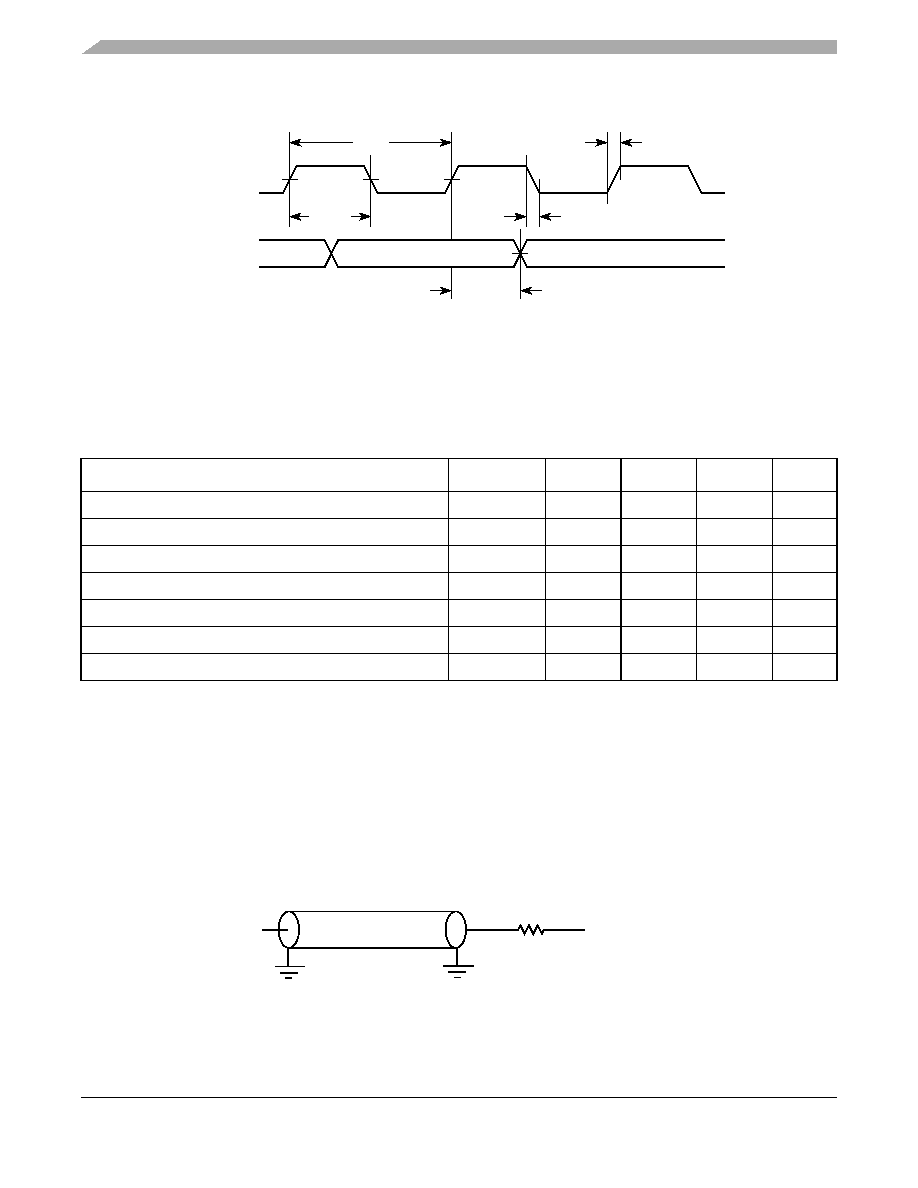
This figure shows the MII transmit AC timing diagram.
Figure 8. MII Transmit AC Timing Diagram
8.2.1.2
MII Receive AC Timing Specifications
This table provides the MII receive AC timing specifications.
This figure provides the AC test load for TSEC.
Figure 9. TSEC AC Test Load
Table 27. MII Receive AC Timing Specifications
At recommended operating conditions with LVDDA/LVDDB/NVDD of 3.3 V ± 0.3 V.
Parameter/Condition
Symbol1
Min
Typ
Max
Unit
RX_CLK clock period 10 Mbps
tMRX
—400
—
ns
RX_CLK clock period 100 Mbps
tMRX
—40—
ns
RX_CLK duty cycle
tMRXH/tMRX
35
—
65
%
RXD[3:0], RX_DV, RX_ER setup time to RX_CLK
tMRDVKH
10.0
—
ns
RXD[3:0], RX_DV, RX_ER hold time to RX_CLK
tMRDXKH
10.0
—
ns
RX_CLK clock rise VIL(min) to VIH(max)
tMRXR
1.0
—
4.0
ns
RX_CLK clock fall time VIH(max) to VIL(min)
tMRXF
1.0
—
4.0
ns
Note:
1. The symbols used for timing specifications follow the pattern of t(first two letters of functional block)(signal)(state)(reference)(state) for
inputs and t(first two letters of functional block)(reference)(state)(signal)(state) for outputs. For example, tMRDVKH symbolizes MII receive
timing (MR) with respect to the time data input signals (D) reach the valid state (V) relative to the tMRX clock reference (K)
going to the high (H) state or setup time. Also, tMRDXKL symbolizes MII receive timing (GR) with respect to the time data
input signals (D) went invalid (X) relative to the tMRX clock reference (K) going to the low (L) state or hold time. Note that, in
general, the clock reference symbol representation is based on three letters representing the clock of a particular functional.
For example, the subscript of tMRX represents the MII (M) receive (RX) clock. For rise and fall times, the latter convention
is used with the appropriate letter: R (rise) or F (fall).
2. The frequency of RX_CLK should not exceed the TX_CLK by more than 300 ppm
TX_CLK
TXD[3:0]
tMTKHDX
tMTX
tMTXH
tMTXR
tMTXF
TX_EN
TX_ER
Output
Z0 = 50
LVDDA/2 or LVDDB/2
RL = 50
相关PDF资料 |
PDF描述 |
|---|---|
| 2-1734798-7 | CONN HOUSING FPC 27POS R/A SMD |
| 487951-4 | 004 1MM FPC TOP HORZ |
| 3-487951-0 | CONN 1MM FPC 30POS R/A SMD |
| 487576-4 | CONN ZIF LINE 12POS TIN |
| 2-1734798-6 | CONN HOUSING FPC 26POS R/A SMD |
相关代理商/技术参数 |
参数描述 |
|---|---|
| KMPC8314CVRAGDA | 功能描述:微处理器 - MPU NON-ENCRYPT RoHS:否 制造商:Atmel 处理器系列:SAMA5D31 核心:ARM Cortex A5 数据总线宽度:32 bit 最大时钟频率:536 MHz 程序存储器大小:32 KB 数据 RAM 大小:128 KB 接口类型:CAN, Ethernet, LIN, SPI,TWI, UART, USB 工作电源电压:1.8 V to 3.3 V 最大工作温度:+ 85 C 安装风格:SMD/SMT 封装 / 箱体:FBGA-324 |
| KMPC8314ECVRAGDA | 功能描述:微处理器 - MPU ENCRYPT RoHS:否 制造商:Atmel 处理器系列:SAMA5D31 核心:ARM Cortex A5 数据总线宽度:32 bit 最大时钟频率:536 MHz 程序存储器大小:32 KB 数据 RAM 大小:128 KB 接口类型:CAN, Ethernet, LIN, SPI,TWI, UART, USB 工作电源电压:1.8 V to 3.3 V 最大工作温度:+ 85 C 安装风格:SMD/SMT 封装 / 箱体:FBGA-324 |
| KMPC8314EVRAGDA | 功能描述:微处理器 - MPU ENCRYPT RoHS:否 制造商:Atmel 处理器系列:SAMA5D31 核心:ARM Cortex A5 数据总线宽度:32 bit 最大时钟频率:536 MHz 程序存储器大小:32 KB 数据 RAM 大小:128 KB 接口类型:CAN, Ethernet, LIN, SPI,TWI, UART, USB 工作电源电压:1.8 V to 3.3 V 最大工作温度:+ 85 C 安装风格:SMD/SMT 封装 / 箱体:FBGA-324 |
| KMPC8314VRAGDA | 功能描述:微处理器 - MPU NON-ENCRYPT RoHS:否 制造商:Atmel 处理器系列:SAMA5D31 核心:ARM Cortex A5 数据总线宽度:32 bit 最大时钟频率:536 MHz 程序存储器大小:32 KB 数据 RAM 大小:128 KB 接口类型:CAN, Ethernet, LIN, SPI,TWI, UART, USB 工作电源电压:1.8 V to 3.3 V 最大工作温度:+ 85 C 安装风格:SMD/SMT 封装 / 箱体:FBGA-324 |
| KMPC8315CVRAGDA | 功能描述:微处理器 - MPU NON-ENCRYPT RoHS:否 制造商:Atmel 处理器系列:SAMA5D31 核心:ARM Cortex A5 数据总线宽度:32 bit 最大时钟频率:536 MHz 程序存储器大小:32 KB 数据 RAM 大小:128 KB 接口类型:CAN, Ethernet, LIN, SPI,TWI, UART, USB 工作电源电压:1.8 V to 3.3 V 最大工作温度:+ 85 C 安装风格:SMD/SMT 封装 / 箱体:FBGA-324 |
发布紧急采购,3分钟左右您将得到回复。