- 您现在的位置:买卖IC网 > PDF目录3945 > KMPC8314EVRAGDA (Freescale Semiconductor)IC MPU POWERQUICC II 620-PBGA PDF资料下载
参数资料
| 型号: | KMPC8314EVRAGDA |
| 厂商: | Freescale Semiconductor |
| 文件页数: | 12/101页 |
| 文件大小: | 0K |
| 描述: | IC MPU POWERQUICC II 620-PBGA |
| 标准包装: | 2 |
| 系列: | MPC83xx |
| 处理器类型: | 32-位 MPC83xx PowerQUICC II Pro |
| 速度: | 400MHz |
| 电压: | 1V |
| 安装类型: | 表面贴装 |
| 封装/外壳: | 620-BBGA 裸露焊盘 |
| 供应商设备封装: | 620-PBGA(29x29) |
| 包装: | 托盘 |
第1页第2页第3页第4页第5页第6页第7页第8页第9页第10页第11页当前第12页第13页第14页第15页第16页第17页第18页第19页第20页第21页第22页第23页第24页第25页第26页第27页第28页第29页第30页第31页第32页第33页第34页第35页第36页第37页第38页第39页第40页第41页第42页第43页第44页第45页第46页第47页第48页第49页第50页第51页第52页第53页第54页第55页第56页第57页第58页第59页第60页第61页第62页第63页第64页第65页第66页第67页第68页第69页第70页第71页第72页第73页第74页第75页第76页第77页第78页第79页第80页第81页第82页第83页第84页第85页第86页第87页第88页第89页第90页第91页第92页第93页第94页第95页第96页第97页第98页第99页第100页第101页
MPC8314E PowerQUICC II Pro Processor Hardware Specifications, Rev. 2
18
Freescale Semiconductor
DDR and DDR2 SDRAM
7.2
DDR and DDR2 SDRAM AC Electrical Characteristics
This section provides the AC electrical characteristics for the DDR and DDR2 SDRAM interface.
7.2.1
DDR and DDR2 SDRAM Input AC Timing Specifications
This table lists the input AC timing specifications for the DDR2 SDRAM (GVDD(typ) = 1.8 V).
This table lists the input AC timing specifications for the DDR SDRAM when GVDD(typ)=2.5 V.
The following two tables list the input AC timing specifications for the DDR SDRAM interface.
Note:
1. The voltage regulator for MVREF must be able to supply up to 500 A current.
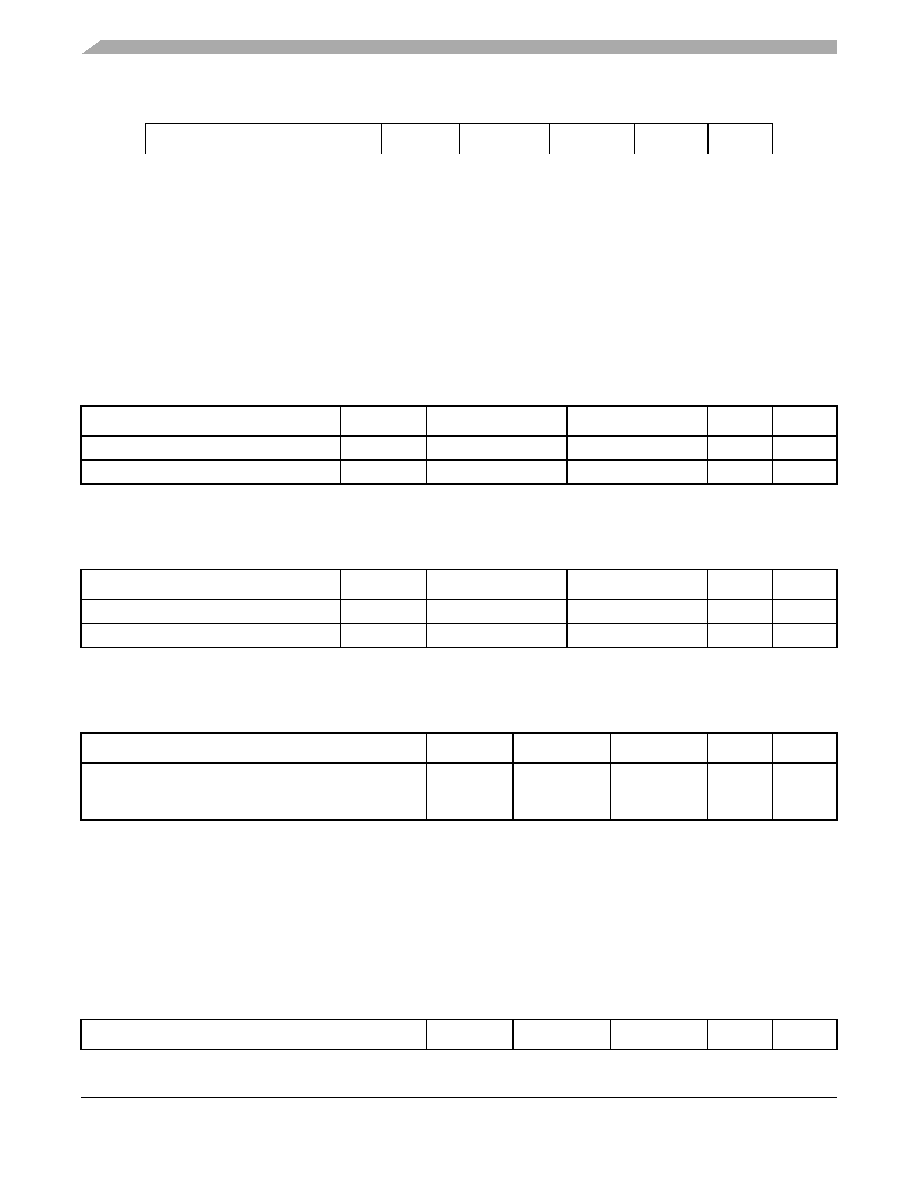
Table 16. DDR2 SDRAM Input AC Timing Specifications for 1.8-V Interface
At recommended operating conditions with GVDD of 1.8V ± 100 mV
Parameter
Symbol
Min
Max
Unit
Note
AC input low voltage
VIL
—
MVREF – 0.45
V
—
AC input high voltage
VIH
MVREF + 0.45
—
V
—
Table 17. DDR SDRAM Input AC Timing Specifications for 2.5 V Interface
At recommended operating conditions with GVDD of 2.5V ± 200 mV
Parameter
Symbol
Min
Max
Unit
Note
AC input low voltage
VIL
—
MVREF – 0.51
V
AC input high voltage
VIH
MVREF + 0.51
—
V
Table 18. DDR2 SDRAM Input AC Timing Specifications
At recommended operating conditions with GVDD of (1.8 V± 100 mV)
Parameter
Symbol
Min
Max
Unit
Note
Controller Skew for MDQS—MDQ
266 MHz
200 MHz
tCISKEW
–875
–1250
875
1250
ps
1, 2, 3
Note:
1. tCISKEW represents the total amount of skew consumed by the controller between MDQS[n] and any corresponding bit to
be captured with MDQS[n]. This should be subtracted from the total timing budget.
2. The amount of skew that can be tolerated from MDQS to a corresponding MDQ signal is called tDISKEW.This can be
determined by the following equation: tDISKEW =+/–(T/4 – abs(tCISKEW)) where T is the clock period and abs(tCISKEW) is
the absolute value of tCISKEW.
3. Memory controller ODT value of 150
is recommended.
Table 19. DDR SDRAM Input AC Timing Specifications
At recommended operating conditions with GVDD of (2.5V ± 200 mV)
Parameter
Symbol
Min
Max
Unit
Note
Table 15. Current Draw Characteristics for MVREF
Parameter / Condition
Symbol
Min
Max
Unit
Note
相关PDF资料 |
PDF描述 |
|---|---|
| KMPC8314ECVRAGDA | IC MPU POWERQUICC II 620-PBGA |
| KMPC8314CVRAGDA | IC MPU POWERQUICC II 620-PBGA |
| KMPC8313ZQAFFB | IC MPU POWERQUICC II 516-PBGA |
| 2-1734798-7 | CONN HOUSING FPC 27POS R/A SMD |
| 487951-4 | 004 1MM FPC TOP HORZ |
相关代理商/技术参数 |
参数描述 |
|---|---|
| KMPC8314VRAGDA | 功能描述:微处理器 - MPU NON-ENCRYPT RoHS:否 制造商:Atmel 处理器系列:SAMA5D31 核心:ARM Cortex A5 数据总线宽度:32 bit 最大时钟频率:536 MHz 程序存储器大小:32 KB 数据 RAM 大小:128 KB 接口类型:CAN, Ethernet, LIN, SPI,TWI, UART, USB 工作电源电压:1.8 V to 3.3 V 最大工作温度:+ 85 C 安装风格:SMD/SMT 封装 / 箱体:FBGA-324 |
| KMPC8315CVRAGDA | 功能描述:微处理器 - MPU NON-ENCRYPT RoHS:否 制造商:Atmel 处理器系列:SAMA5D31 核心:ARM Cortex A5 数据总线宽度:32 bit 最大时钟频率:536 MHz 程序存储器大小:32 KB 数据 RAM 大小:128 KB 接口类型:CAN, Ethernet, LIN, SPI,TWI, UART, USB 工作电源电压:1.8 V to 3.3 V 最大工作温度:+ 85 C 安装风格:SMD/SMT 封装 / 箱体:FBGA-324 |
| KMPC8315ECVRAGDA | 功能描述:微处理器 - MPU ENCRYPT RoHS:否 制造商:Atmel 处理器系列:SAMA5D31 核心:ARM Cortex A5 数据总线宽度:32 bit 最大时钟频率:536 MHz 程序存储器大小:32 KB 数据 RAM 大小:128 KB 接口类型:CAN, Ethernet, LIN, SPI,TWI, UART, USB 工作电源电压:1.8 V to 3.3 V 最大工作温度:+ 85 C 安装风格:SMD/SMT 封装 / 箱体:FBGA-324 |
| KMPC8315EVRAGDA | 功能描述:微处理器 - MPU ENCRYPT RoHS:否 制造商:Atmel 处理器系列:SAMA5D31 核心:ARM Cortex A5 数据总线宽度:32 bit 最大时钟频率:536 MHz 程序存储器大小:32 KB 数据 RAM 大小:128 KB 接口类型:CAN, Ethernet, LIN, SPI,TWI, UART, USB 工作电源电压:1.8 V to 3.3 V 最大工作温度:+ 85 C 安装风格:SMD/SMT 封装 / 箱体:FBGA-324 |
| KMPC8315VRAGDA | 功能描述:微处理器 - MPU NON-ENCRYPT RoHS:否 制造商:Atmel 处理器系列:SAMA5D31 核心:ARM Cortex A5 数据总线宽度:32 bit 最大时钟频率:536 MHz 程序存储器大小:32 KB 数据 RAM 大小:128 KB 接口类型:CAN, Ethernet, LIN, SPI,TWI, UART, USB 工作电源电压:1.8 V to 3.3 V 最大工作温度:+ 85 C 安装风格:SMD/SMT 封装 / 箱体:FBGA-324 |
发布紧急采购,3分钟左右您将得到回复。