- 您现在的位置:买卖IC网 > PDF目录3945 > KMPC8315CVRAGDA (Freescale Semiconductor)IC MPU POWERQUICC II 620-PBGA PDF资料下载
参数资料
| 型号: | KMPC8315CVRAGDA |
| 厂商: | Freescale Semiconductor |
| 文件页数: | 16/106页 |
| 文件大小: | 0K |
| 描述: | IC MPU POWERQUICC II 620-PBGA |
| 标准包装: | 2 |
| 系列: | MPC83xx |
| 处理器类型: | 32-位 MPC83xx PowerQUICC II Pro |
| 速度: | 400MHz |
| 电压: | 1V |
| 安装类型: | 表面贴装 |
| 封装/外壳: | 620-BBGA 裸露焊盘 |
| 供应商设备封装: | 620-PBGA(29x29) |
| 包装: | 托盘 |
第1页第2页第3页第4页第5页第6页第7页第8页第9页第10页第11页第12页第13页第14页第15页当前第16页第17页第18页第19页第20页第21页第22页第23页第24页第25页第26页第27页第28页第29页第30页第31页第32页第33页第34页第35页第36页第37页第38页第39页第40页第41页第42页第43页第44页第45页第46页第47页第48页第49页第50页第51页第52页第53页第54页第55页第56页第57页第58页第59页第60页第61页第62页第63页第64页第65页第66页第67页第68页第69页第70页第71页第72页第73页第74页第75页第76页第77页第78页第79页第80页第81页第82页第83页第84页第85页第86页第87页第88页第89页第90页第91页第92页第93页第94页第95页第96页第97页第98页第99页第100页第101页第102页第103页第104页第105页第106页
MPC8315E PowerQUICC II Pro Processor Hardware Specifications, Rev. 2
Freescale Semiconductor
17
RESET Initialization
6
RESET Initialization
This section describes the DC and AC electrical specifications for the reset initialization timing and
electrical requirements of the MPC8315E.
6.1
RESET DC Electrical Characteristics
This table provides the DC electrical characteristics for the RESET pins of the MPC8315E.
6.2
RESET AC Electrical Characteristics
This table provides the reset initialization AC timing specifications of the MPC8315E.
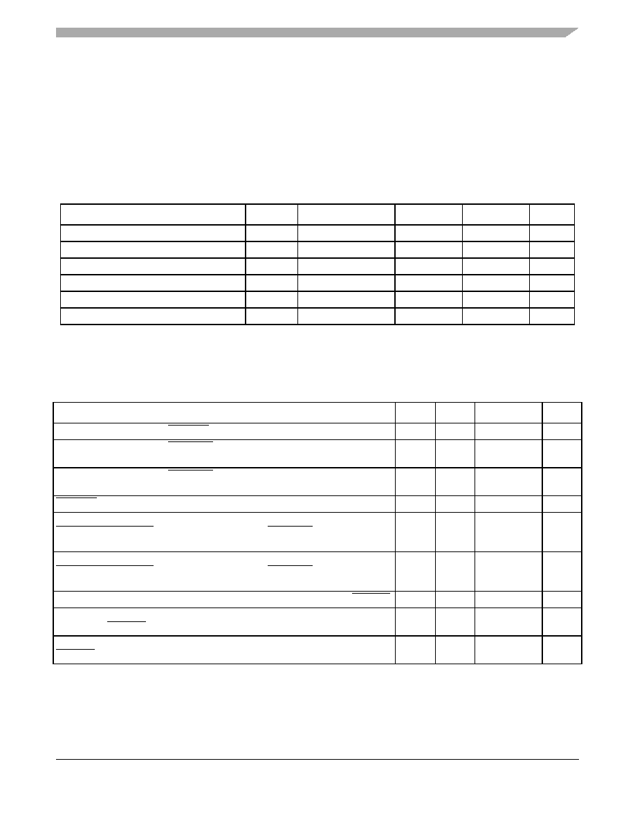
Table 8. RESET Pins DC Electrical Characteristics
Characteristic
Symbol
Condition
Min
Max
Unit
Input high voltage
VIH
—
2.0
NVDD + 0.3
V
Input low voltage
VIL
—–0.3
0.8
V
Input current
IIN
0 V
V
IN NVDD
—
±5
A
Output high voltage
VOH
IOH = –8.0 mA
2.4
—
V
Output low voltage
VOL
IOL = 8.0 mA
—
0.5
V
Output low voltage
VOL
IOL = 3.2 mA
—
0.4
V
Table 9. RESET Initialization Timing Specifications
Parameter/Condition
Min
Max
Unit
Note
Required assertion time of HRESET to activate reset flow
32
—
tPCI_SYNC_IN
1
Required assertion time of PORESET with stable clock applied to SYS_CLK_IN
when the device is in PCI host mode
32
—
tSYS_CLK_IN
2
Required assertion time of PORESET with stable clock applied to PCI_SYNC_IN
when the device is in PCI agent mode
32
—
tPCI_SYNC_IN
1
HRESET assertion (output)
512
—
tPCI_SYNC_IN
1
Input setup time for POR configuration signals (CFG_RESET_SOURCE[0:3] and
CFG_SYS_CLKIN_DIV) with respect to negation of PORESET when the device is
in PCI host mode
4—
tSYS_CLK_IN
2, 4
Input setup time for POR configuration signals (CFG_RESET_SOURCE[0:3] and
CFG_SYS_CLKIN_DIV) with respect to negation of PORESET when the device is
in PCI agent mode
4—
tPCI_SYNC_IN
1
Input hold time for POR configuration signals with respect to negation of HRESET
0—
ns
—
Time for the device to turn off POR configuration signals with respect to the
assertion of HRESET
—4
ns
3
Time for the device to turn on POR config signals with respect to the negation of
HRESET
1—
tPCI_SYNC_IN
1, 3
相关PDF资料 |
PDF描述 |
|---|---|
| KMPC8314EVRAGDA | IC MPU POWERQUICC II 620-PBGA |
| KMPC8314ECVRAGDA | IC MPU POWERQUICC II 620-PBGA |
| KMPC8314CVRAGDA | IC MPU POWERQUICC II 620-PBGA |
| KMPC8313ZQAFFB | IC MPU POWERQUICC II 516-PBGA |
| 2-1734798-7 | CONN HOUSING FPC 27POS R/A SMD |
相关代理商/技术参数 |
参数描述 |
|---|---|
| KMPC8315ECVRAGDA | 功能描述:微处理器 - MPU ENCRYPT RoHS:否 制造商:Atmel 处理器系列:SAMA5D31 核心:ARM Cortex A5 数据总线宽度:32 bit 最大时钟频率:536 MHz 程序存储器大小:32 KB 数据 RAM 大小:128 KB 接口类型:CAN, Ethernet, LIN, SPI,TWI, UART, USB 工作电源电压:1.8 V to 3.3 V 最大工作温度:+ 85 C 安装风格:SMD/SMT 封装 / 箱体:FBGA-324 |
| KMPC8315EVRAGDA | 功能描述:微处理器 - MPU ENCRYPT RoHS:否 制造商:Atmel 处理器系列:SAMA5D31 核心:ARM Cortex A5 数据总线宽度:32 bit 最大时钟频率:536 MHz 程序存储器大小:32 KB 数据 RAM 大小:128 KB 接口类型:CAN, Ethernet, LIN, SPI,TWI, UART, USB 工作电源电压:1.8 V to 3.3 V 最大工作温度:+ 85 C 安装风格:SMD/SMT 封装 / 箱体:FBGA-324 |
| KMPC8315VRAGDA | 功能描述:微处理器 - MPU NON-ENCRYPT RoHS:否 制造商:Atmel 处理器系列:SAMA5D31 核心:ARM Cortex A5 数据总线宽度:32 bit 最大时钟频率:536 MHz 程序存储器大小:32 KB 数据 RAM 大小:128 KB 接口类型:CAN, Ethernet, LIN, SPI,TWI, UART, USB 工作电源电压:1.8 V to 3.3 V 最大工作温度:+ 85 C 安装风格:SMD/SMT 封装 / 箱体:FBGA-324 |
| KMPC8321CVRADDC | 功能描述:微处理器 - MPU 8321 NOPB PBGA W/O ENCR RoHS:否 制造商:Atmel 处理器系列:SAMA5D31 核心:ARM Cortex A5 数据总线宽度:32 bit 最大时钟频率:536 MHz 程序存储器大小:32 KB 数据 RAM 大小:128 KB 接口类型:CAN, Ethernet, LIN, SPI,TWI, UART, USB 工作电源电压:1.8 V to 3.3 V 最大工作温度:+ 85 C 安装风格:SMD/SMT 封装 / 箱体:FBGA-324 |
| KMPC8321CVRAFDC | 功能描述:微处理器 - MPU 8321 NOPB PBGA W/O ENCR RoHS:否 制造商:Atmel 处理器系列:SAMA5D31 核心:ARM Cortex A5 数据总线宽度:32 bit 最大时钟频率:536 MHz 程序存储器大小:32 KB 数据 RAM 大小:128 KB 接口类型:CAN, Ethernet, LIN, SPI,TWI, UART, USB 工作电源电压:1.8 V to 3.3 V 最大工作温度:+ 85 C 安装风格:SMD/SMT 封装 / 箱体:FBGA-324 |
发布紧急采购,3分钟左右您将得到回复。