参数资料
| 型号: | KMPC8323VRAFDC |
| 厂商: | Freescale Semiconductor |
| 文件页数: | 37/82页 |
| 文件大小: | 0K |
| 描述: | IC MPU 516-PBGA |
| 标准包装: | 2 |
| 系列: | MPC83xx |
| 处理器类型: | 32-位 MPC83xx PowerQUICC II Pro |
| 速度: | 333MHz |
| 电压: | 1V |
| 安装类型: | 表面贴装 |
| 封装/外壳: | 516-BBGA |
| 供应商设备封装: | 516-FPBGA(27x27) |
| 包装: | 托盘 |
第1页第2页第3页第4页第5页第6页第7页第8页第9页第10页第11页第12页第13页第14页第15页第16页第17页第18页第19页第20页第21页第22页第23页第24页第25页第26页第27页第28页第29页第30页第31页第32页第33页第34页第35页第36页当前第37页第38页第39页第40页第41页第42页第43页第44页第45页第46页第47页第48页第49页第50页第51页第52页第53页第54页第55页第56页第57页第58页第59页第60页第61页第62页第63页第64页第65页第66页第67页第68页第69页第70页第71页第72页第73页第74页第75页第76页第77页第78页第79页第80页第81页第82页
MPC8323E PowerQUICC II Pro Integrated Communications Processor Family Hardware Specifications, Rev. 4
42
Freescale Semiconductor
TDM/SI
17.2
TDM/SI AC Timing Specifications
Table 47 provides the TDM/SI input and output AC timing specifications.
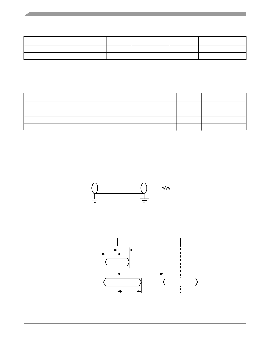
Figure 33 provides the AC test load for the TDM/SI.
Figure 33. TDM/SI AC Test Load
reference the rising edge of the clock, these AC timing diagrams also apply when the falling edge is the
active edge.
Figure 34. TDM/SI AC Timing (External Clock) Diagram
Input low voltage
VIL
—
–0.3
0.8
V
Input current
IIN
0 V
≤ VIN ≤ OVDD
—±5
μA
Table 47. TDM/SI AC Timing Specifications1
Characteristic
Symbol2
Min
Max
Unit
TDM/SI outputs—External clock delay
tSEKHOV
212
ns
TDM/SI outputs—External clock High Impedance
tSEKHOX
210
ns
TDM/SI inputs—External clock input setup time
tSEIVKH
5—
ns
TDM/SI inputs—External clock input hold time
tSEIXKH
2—
ns
Notes:
1. Output specifications are measured from the 50% level of the rising edge of CLKIN to the 50% level of the signal. Timings
are measured at the pin.
2. The symbols used for timing specifications follow the pattern of t(first two letters of functional block)(signal)(state)(reference)(state) for
inputs and t(first two letters of functional block)(reference)(state)(signal)(state) for outputs. For example, tSEKHOX symbolizes the TDM/SI
outputs external timing (SE) for the time tTDM/SI memory clock reference (K) goes from the high state (H) until outputs (O)
are invalid (X).
Table 46. TDM/SI DC Electrical Characteristics (continued)
Characteristic
Symbol
Condition
Min
Max
Unit
Output
Z0 = 50 Ω
OVDD/2
RL = 50 Ω
TDM/SICLK (Input)
tSEIXKH
tSEIVKH
tSEKHOV
Input Signals:
TDM/SI
(See Note)
Output Signals:
TDM/SI
(See Note)
Note: The clock edge is selectable on TDM/SI.
tSEKHOX
相关PDF资料 |
PDF描述 |
|---|---|
| IDT70V3599S166BCG | IC SRAM 4MBIT 166MHZ 256BGA |
| KMPC8321EVRAFDC | IC MPU 516-PBGA |
| KMPC8321VRADDC | IC MPU 516-PBGA |
| KMPC8321VRAFDC | IC MPU 516-PBGA |
| IDT70V3319S166BCG | IC SRAM 4MBIT 166MHZ 256BGA |
相关代理商/技术参数 |
参数描述 |
|---|---|
| KMPC8323ZQADDC | 功能描述:微处理器 - MPU 8323 PBGA W/O ENCR RoHS:否 制造商:Atmel 处理器系列:SAMA5D31 核心:ARM Cortex A5 数据总线宽度:32 bit 最大时钟频率:536 MHz 程序存储器大小:32 KB 数据 RAM 大小:128 KB 接口类型:CAN, Ethernet, LIN, SPI,TWI, UART, USB 工作电源电压:1.8 V to 3.3 V 最大工作温度:+ 85 C 安装风格:SMD/SMT 封装 / 箱体:FBGA-324 |
| KMPC8323ZQAFDC | 功能描述:微处理器 - MPU 8323 PBGA W/O ENCR RoHS:否 制造商:Atmel 处理器系列:SAMA5D31 核心:ARM Cortex A5 数据总线宽度:32 bit 最大时钟频率:536 MHz 程序存储器大小:32 KB 数据 RAM 大小:128 KB 接口类型:CAN, Ethernet, LIN, SPI,TWI, UART, USB 工作电源电压:1.8 V to 3.3 V 最大工作温度:+ 85 C 安装风格:SMD/SMT 封装 / 箱体:FBGA-324 |
| KMPC8343CVRAGDB | 功能描述:微处理器 - MPU 8347 PBGA NOPB W/O ENC RoHS:否 制造商:Atmel 处理器系列:SAMA5D31 核心:ARM Cortex A5 数据总线宽度:32 bit 最大时钟频率:536 MHz 程序存储器大小:32 KB 数据 RAM 大小:128 KB 接口类型:CAN, Ethernet, LIN, SPI,TWI, UART, USB 工作电源电压:1.8 V to 3.3 V 最大工作温度:+ 85 C 安装风格:SMD/SMT 封装 / 箱体:FBGA-324 |
| KMPC8343CZQAGD | 功能描述:IC MPU PWRQUICC II 620-PBGA RoHS:否 类别:集成电路 (IC) >> 嵌入式 - 微处理器 系列:MPC83xx 标准包装:2 系列:MPC8xx 处理器类型:32-位 MPC8xx PowerQUICC 特点:- 速度:133MHz 电压:3.3V 安装类型:表面贴装 封装/外壳:357-BBGA 供应商设备封装:357-PBGA(25x25) 包装:托盘 |
| KMPC8343CZQAGDB | 功能描述:微处理器 - MPU 8347 PBGA W/O ENC W/ PB RoHS:否 制造商:Atmel 处理器系列:SAMA5D31 核心:ARM Cortex A5 数据总线宽度:32 bit 最大时钟频率:536 MHz 程序存储器大小:32 KB 数据 RAM 大小:128 KB 接口类型:CAN, Ethernet, LIN, SPI,TWI, UART, USB 工作电源电压:1.8 V to 3.3 V 最大工作温度:+ 85 C 安装风格:SMD/SMT 封装 / 箱体:FBGA-324 |
发布紧急采购,3分钟左右您将得到回复。