- 您现在的位置:买卖IC网 > PDF目录3960 > KMPC8548EHXAUJ (Freescale Semiconductor)IC MPU PWRQUICC III 783-FCCBGA PDF资料下载
参数资料
| 型号: | KMPC8548EHXAUJ |
| 厂商: | Freescale Semiconductor |
| 文件页数: | 55/151页 |
| 文件大小: | 0K |
| 描述: | IC MPU PWRQUICC III 783-FCCBGA |
| 标准包装: | 2 |
| 系列: | MPC85xx |
| 处理器类型: | 32-位 MPC85xx PowerQUICC III |
| 速度: | 1.333GHz |
| 电压: | 1.1V |
| 安装类型: | 表面贴装 |
| 封装/外壳: | 783-BBGA,FCBGA |
| 供应商设备封装: | 783-FCPBGA(29x29) |
| 包装: | 托盘 |
第1页第2页第3页第4页第5页第6页第7页第8页第9页第10页第11页第12页第13页第14页第15页第16页第17页第18页第19页第20页第21页第22页第23页第24页第25页第26页第27页第28页第29页第30页第31页第32页第33页第34页第35页第36页第37页第38页第39页第40页第41页第42页第43页第44页第45页第46页第47页第48页第49页第50页第51页第52页第53页第54页当前第55页第56页第57页第58页第59页第60页第61页第62页第63页第64页第65页第66页第67页第68页第69页第70页第71页第72页第73页第74页第75页第76页第77页第78页第79页第80页第81页第82页第83页第84页第85页第86页第87页第88页第89页第90页第91页第92页第93页第94页第95页第96页第97页第98页第99页第100页第101页第102页第103页第104页第105页第106页第107页第108页第109页第110页第111页第112页第113页第114页第115页第116页第117页第118页第119页第120页第121页第122页第123页第124页第125页第126页第127页第128页第129页第130页第131页第132页第133页第134页第135页第136页第137页第138页第139页第140页第141页第142页第143页第144页第145页第146页第147页第148页第149页第150页第151页
MPC8548E PowerQUICC III Integrated Processor Hardware Specifications, Rev. 9
148
Freescale Semiconductor
Document Revision History
24 Document Revision History
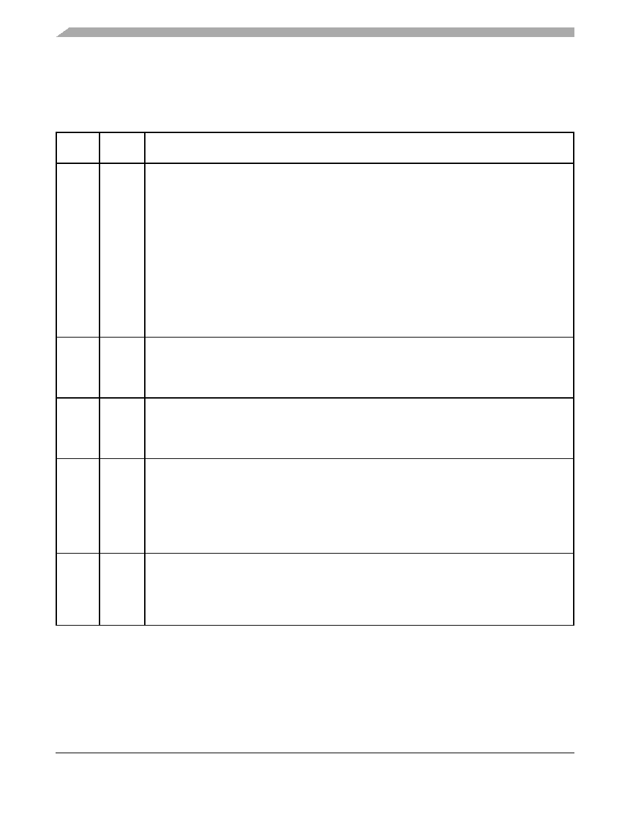
The following table provides a revision history for this hardware specification.
Table 88. Document Revision History
Rev.
Number
Date
Substantive Change(s)
9
02/2012
Updated Section 21.2, “Thermal for Version 2.1.1, 2.1.2, and 2.1.3 Silicon FC-PBGA with Full Lid and
Version 3.1.x Silicon with Stamped Lid,” with version 3.0 silicon information.
Updated Table 87, “Part Numbering Nomenclature,” with version 3.0 silicon information.
Removed table 11.
Updated the title of Section 21.2, “Thermal for Version 2.1.1, 2.1.2, and 2.1.3 Silicon FC-PBGA with
Full Lid and Version 3.1.x Silicon with Stamped Lid” to include Thermal Version 2.1.3 and Version 3.1.x
Corrected the leaded Solder Ball composition in Table 70, “Package Parameters”
Updated Table 87, “Part Numbering Nomenclature,” with Version 3.1.x silicon information.
Updated the Min and Max value of TDO in the valid times row of Table 44, “JTAG AC Timing
Specifications (Independent of SYSCLK)1” from 4 and 25 to 2 and 10 respectively .
8
04/2011
“MPC8545E Pinout Listing,” and Table 74, “MPC8543E Pinout Listing,” to reflect that the TDO signal
is not driven during HRSET* assertion.
Updated Table 87, “Part Numbering Nomenclature” with Ver. 2.1.3 silicon information.
7
09/2010
In Table 37, “MII Management AC Timing Specifications, modified the fifth row from “MDC to MDIO
delay tMDKHDX (16 × tptb_clk × 8) – 3 — (16 × tptb_clk × 8) + 3” to “MDC to MDIO delay tMDKHDX
(16 × tCCB × 8) – 3 — (16 × tCCB × 8) + 3.”
FC-CBGA and FC-PBGA with Full Lid and figure notes.
6
12/2009
In Section 5.1, “Power-On Ramp Rate” added explanation that Power-On Ramp Rate is required to
avoid falsely triggering ESD circuitry.
In Table 13 changed required ramp rate from 545 V/s for MVREF and VDD/XVDD/SVDD to 3500 V/s
for MVREF and 4000 V/s for VDD.
In Table 13 deleted ramp rate requirement for XVDD/SVDD.
In Table 13 footnote 1 changed voltage range of concern from 0–400 mV to 20–500mV.
In Table 13 added footnote 2 explaining that VDD voltage ramp rate is intended to control ramp rate of
AVDD pins.
5
10/2009
In Table 27, “GMII Receive AC Timing Specifications,” changed duty cycle specification from 40/60 to
35/75 for RX_CLK duty cycle.
Updated tMDKHDX in Table 37, “MII Management AC Timing Specifications.”
Added a reference to Revision 2.1.2.
Updated Table 55, “MII Management AC Timing Specifications.”
Added Section 5.1, “Power-On Ramp Rate.”
相关PDF资料 |
PDF描述 |
|---|---|
| 396-012-521-204 | CARD EDGE 12POS DL .125X.25 BLK |
| IDT70V631S12PRFI8 | IC SRAM 4MBIT 12NS 128TQFP |
| 396-012-521-202 | CARD EDGE 12POS DL .125X.25 BLK |
| 396-012-521-201 | CARD EDGE 12POS DL .125X.25 BLK |
| KMPC8548EHXAQG | IC MPU PWRQUICC III 783-FCCBGA |
相关代理商/技术参数 |
参数描述 |
|---|---|
| KMPC8548EPXAUJB | 功能描述:微处理器 - MPU FG PQ38 8548 RoHS:否 制造商:Atmel 处理器系列:SAMA5D31 核心:ARM Cortex A5 数据总线宽度:32 bit 最大时钟频率:536 MHz 程序存储器大小:32 KB 数据 RAM 大小:128 KB 接口类型:CAN, Ethernet, LIN, SPI,TWI, UART, USB 工作电源电压:1.8 V to 3.3 V 最大工作温度:+ 85 C 安装风格:SMD/SMT 封装 / 箱体:FBGA-324 |
| KMPC8548EPXAVHB | 功能描述:微处理器 - MPU FG PQ38 8548 RoHS:否 制造商:Atmel 处理器系列:SAMA5D31 核心:ARM Cortex A5 数据总线宽度:32 bit 最大时钟频率:536 MHz 程序存储器大小:32 KB 数据 RAM 大小:128 KB 接口类型:CAN, Ethernet, LIN, SPI,TWI, UART, USB 工作电源电压:1.8 V to 3.3 V 最大工作温度:+ 85 C 安装风格:SMD/SMT 封装 / 箱体:FBGA-324 |
| KMPC8548EVTAUJB | 功能描述:微处理器 - MPU FG PQ38 8548 PB Free RoHS:否 制造商:Atmel 处理器系列:SAMA5D31 核心:ARM Cortex A5 数据总线宽度:32 bit 最大时钟频率:536 MHz 程序存储器大小:32 KB 数据 RAM 大小:128 KB 接口类型:CAN, Ethernet, LIN, SPI,TWI, UART, USB 工作电源电压:1.8 V to 3.3 V 最大工作温度:+ 85 C 安装风格:SMD/SMT 封装 / 箱体:FBGA-324 |
| KMPC8548EVTAUJC | 功能描述:微处理器 - MPU PQ38 8548 RoHS:否 制造商:Atmel 处理器系列:SAMA5D31 核心:ARM Cortex A5 数据总线宽度:32 bit 最大时钟频率:536 MHz 程序存储器大小:32 KB 数据 RAM 大小:128 KB 接口类型:CAN, Ethernet, LIN, SPI,TWI, UART, USB 工作电源电压:1.8 V to 3.3 V 最大工作温度:+ 85 C 安装风格:SMD/SMT 封装 / 箱体:FBGA-324 |
| KMPC8548EVTAVHB | 功能描述:微处理器 - MPU FG PQ38 8548 PB Free RoHS:否 制造商:Atmel 处理器系列:SAMA5D31 核心:ARM Cortex A5 数据总线宽度:32 bit 最大时钟频率:536 MHz 程序存储器大小:32 KB 数据 RAM 大小:128 KB 接口类型:CAN, Ethernet, LIN, SPI,TWI, UART, USB 工作电源电压:1.8 V to 3.3 V 最大工作温度:+ 85 C 安装风格:SMD/SMT 封装 / 箱体:FBGA-324 |
发布紧急采购,3分钟左右您将得到回复。