- 您现在的位置:买卖IC网 > PDF目录3980 > KMPC885VR133 (Freescale Semiconductor)IC MPU POWERQUICC 133MHZ 357PBGA PDF资料下载
参数资料
| 型号: | KMPC885VR133 |
| 厂商: | Freescale Semiconductor |
| 文件页数: | 8/87页 |
| 文件大小: | 0K |
| 描述: | IC MPU POWERQUICC 133MHZ 357PBGA |
| 标准包装: | 2 |
| 系列: | MPC8xx |
| 处理器类型: | 32-位 MPC8xx PowerQUICC |
| 速度: | 133MHz |
| 电压: | 3.3V |
| 安装类型: | 表面贴装 |
| 封装/外壳: | 357-BBGA |
| 供应商设备封装: | 357-PBGA(25x25) |
| 包装: | 托盘 |
第1页第2页第3页第4页第5页第6页第7页当前第8页第9页第10页第11页第12页第13页第14页第15页第16页第17页第18页第19页第20页第21页第22页第23页第24页第25页第26页第27页第28页第29页第30页第31页第32页第33页第34页第35页第36页第37页第38页第39页第40页第41页第42页第43页第44页第45页第46页第47页第48页第49页第50页第51页第52页第53页第54页第55页第56页第57页第58页第59页第60页第61页第62页第63页第64页第65页第66页第67页第68页第69页第70页第71页第72页第73页第74页第75页第76页第77页第78页第79页第80页第81页第82页第83页第84页第85页第86页第87页
MPC885/MPC880 PowerQUICC Hardware Specifications, Rev. 7
16
Freescale Semiconductor
Layout Practices
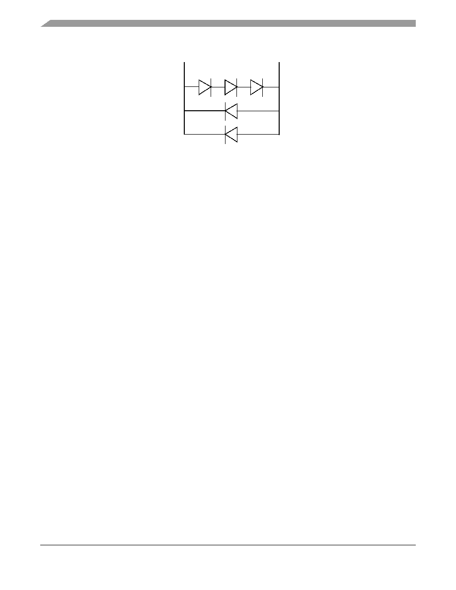
Figure 5. Example Voltage Sequencing Circuit
9
Layout Practices
Each VDD pin on the MPC885/MPC880 should be provided with a low-impedance path to the board’s
supply. Each GND pin should likewise be provided with a low-impedance path to ground. The power
supply pins drive distinct groups of logic on chip. The VDD power supply should be bypassed to ground
using at least four 0.1 F by-pass capacitors located as close as possible to the four sides of the package.
Each board designed should be characterized and additional appropriate decoupling capacitors should be
used if required. The capacitor leads and associated printed-circuit traces connecting to chip VDD and
GND should be kept to less than half an inch per capacitor lead. At a minimum, a four-layer board
employing two inner layers as VDD and GND planes should be used.
All output pins on the MPC885/MPC880 have fast rise and fall times. Printed-circuit (PC) trace
interconnection length should be minimized in order to minimize undershoot and reflections caused by
these fast output switching times. This recommendation particularly applies to the address and data buses.
Maximum PC trace lengths of six inches are recommended. Capacitance calculations should consider all
device loads as well as parasitic capacitances due to the PC traces. Attention to proper PCB layout and
bypassing becomes especially critical in systems with higher capacitive loads because these loads create
higher transient currents in the VDD and GND circuits. Pull up all unused inputs or signals that will be
inputs during reset. Special care should be taken to minimize the noise levels on the PLL supply pins. For
more information, please refer to the MPC885 PowerQUICC Family Reference Manual, Section 14.4.3,
“Clock Synthesizer Power (VDDSYN, VSSSYN, VSSSYN1).”
10 Bus Signal Timing
The maximum bus speed supported by the MPC885/MPC880 is 80 MHz. Higher-speed parts must be
operated in half-speed bus mode (for example, an MPC885/MPC880 used at 133 MHz must be configured
for a 66 MHz bus). Table 7 shows the frequency ranges for standard part frequencies in 1:1 bus mode, and
Table 8 shows the frequency ranges for standard part frequencies in 2:1 bus mode.
VDDH
VDDL
1N5820
MUR420
相关PDF资料 |
PDF描述 |
|---|---|
| HSC50DTEN | CONN EDGECARD 100POS .100 EYELET |
| KMPC885CZP66 | IC MPU POWERQUICC 66MHZ 357PBGA |
| KMPC885CZP133 | IC MPU POWERQUICC 133MHZ 357PBGA |
| HSC50DTEH | CONN EDGECARD 100POS .100 EYELET |
| KMPC885CVR66 | IC MPU POWERQUICC 66MHZ 357PBGA |
相关代理商/技术参数 |
参数描述 |
|---|---|
| KMPC885VR66 | 功能描述:微处理器 - MPU PQ I HIP6W DUET RoHS:否 制造商:Atmel 处理器系列:SAMA5D31 核心:ARM Cortex A5 数据总线宽度:32 bit 最大时钟频率:536 MHz 程序存储器大小:32 KB 数据 RAM 大小:128 KB 接口类型:CAN, Ethernet, LIN, SPI,TWI, UART, USB 工作电源电压:1.8 V to 3.3 V 最大工作温度:+ 85 C 安装风格:SMD/SMT 封装 / 箱体:FBGA-324 |
| KMPC885VR80 | 功能描述:微处理器 - MPU PQ I HIP6W DUET RoHS:否 制造商:Atmel 处理器系列:SAMA5D31 核心:ARM Cortex A5 数据总线宽度:32 bit 最大时钟频率:536 MHz 程序存储器大小:32 KB 数据 RAM 大小:128 KB 接口类型:CAN, Ethernet, LIN, SPI,TWI, UART, USB 工作电源电压:1.8 V to 3.3 V 最大工作温度:+ 85 C 安装风格:SMD/SMT 封装 / 箱体:FBGA-324 |
| KMPC885ZP133 | 功能描述:微处理器 - MPU PQ I HIP6W DUET RoHS:否 制造商:Atmel 处理器系列:SAMA5D31 核心:ARM Cortex A5 数据总线宽度:32 bit 最大时钟频率:536 MHz 程序存储器大小:32 KB 数据 RAM 大小:128 KB 接口类型:CAN, Ethernet, LIN, SPI,TWI, UART, USB 工作电源电压:1.8 V to 3.3 V 最大工作温度:+ 85 C 安装风格:SMD/SMT 封装 / 箱体:FBGA-324 |
| KMPC885ZP66 | 制造商:FREESCALE 制造商全称:Freescale Semiconductor, Inc 功能描述:Hardware Specifications |
| KMPC885ZP80 | 功能描述:微处理器 - MPU PQ I HIP6W DUET RoHS:否 制造商:Atmel 处理器系列:SAMA5D31 核心:ARM Cortex A5 数据总线宽度:32 bit 最大时钟频率:536 MHz 程序存储器大小:32 KB 数据 RAM 大小:128 KB 接口类型:CAN, Ethernet, LIN, SPI,TWI, UART, USB 工作电源电压:1.8 V to 3.3 V 最大工作温度:+ 85 C 安装风格:SMD/SMT 封装 / 箱体:FBGA-324 |
发布紧急采购,3分钟左右您将得到回复。