- 您现在的位置:买卖IC网 > PDF目录374376 > KPF201G01 (KEC Holdings) Semiconductor Pressure Sensor PDF资料下载
参数资料
| 型号: | KPF201G01 |
| 厂商: | KEC Holdings |
| 英文描述: | Semiconductor Pressure Sensor |
| 中文描述: | 半导体压力传感器 |
| 文件页数: | 4/4页 |
| 文件大小: | 540K |
| 代理商: | KPF201G01 |
2007. 6. 15
4/4
KPF500G01 ~ KPF102G01
Revision No :9
Note
1. Mounting on printed circuit boards
When mounting a transistor on a printed circuit, it is assumed that
lead wires will be processed or reformed due to space limitation or
relations with other components. Even if no such special
processing reforming is conducted exercise care on the following
points :
(a) Make the spaces of lead wire inserting holes on the printed
circuit board the same as those of lead wires on a transistor.
(b) Even if The spaces are not the same, do not pull the lead
wires or push heavily against the sensor element.
(c) Use a spacer for form a lead maintain space between a sensor
and a printed circuit board, rather than closely contacting
them with each other.
(d) When forming a lead prior to mounting onto a board
- Bend the lead at a point 3mm or more apart from the
body(Lead root).
- Bend one lead wire after securing the other lead wire. (near
the main body)
- Keep space between the sensor main body and and a fixing
jig.
- When bending the lead along the jig, be careful not to
damage it with an edge of the jig.
- Follow other precautions described in respective standard
(e) When mounting a sensor onto a heat sink
- Use the specified accessory.
- Drill threaded holes on the heat kink as per specifications
and keep the surface free from burrs and undulations.
- Use KEC’s recommended silicon grease.
- Tighten the screw within the specified torque.
- Never apply a pneumatic screwdriver to a transistor main
body.
(f) Do not bend or stretch the lead wires repeatedly.
When pulling in the axial directions, apply 500g or 600g
power, depending on the shapes of lead wires.
2. Soldering
When soldering a sensor to a printed circuit board, the soldering
temperature is usually so high that it adversely affects the sensor.
Normally, tests are conducted at a soldering temperature of 265
for 10 seconds or 300
for 3 seconds. Be sure to complete
soldering procedures under these conditions of temperature and
time.
Be careful to select a type of flux that will neither corrode the
lead wires nor affect the electrical characteristics of a sensor.
The basic precautions for soldering procedures are as follows :
(a) Complete soldering procedures in a time as short as possible.
(b) Do not apply stress to a sensor after soldering by correcting
or modifying its location or direction.
(c) For a sensor employing a heat sink, mount it on the heat sink
first: then solder this unit to a printed circuit board after
confirming that it is fully secured.
(d) Do not directly solder the heat-radiating portion of a sensor
to a printed circuit board.
(e) In flow solder jobs, sensors are apt to float on the solder due
to solder surface tension. When adjusting the locations of
sensor, be careful not to apply excessive stress to the roots of
the sensor lead wires.
(f) When using a soldering iron select those which have less
leakage, and be sure to ground the soldering iron.
3. Cleaning a circuit board
After soldering, circuit boards must be cleaned to remove flux.
Observe the following precautions while cleaning them
(a) When cleaning circuit boards to remove flux, make sure that
no residual reactive ions such as Na or Cl ions remain. Note
that organic solvents react with water to generate hydrogen
chloride and other corrosive gases which can degrade device
performance.
(b) Do not rub the indication marks with a brush or one
’
s fingers
when cleaning or while a cleaning agent is applied to the
markings.
(c) There are ultrasonic wave cleaning methods which offer a
high cleaning effect within a short time. Since there methods
involve a complicated combination of factors such as the
cleaning bath size, ultrasonic wave vibrator output, and
printed circuit board mounting method, there is fear that the
service life of airtight seal-type sensors may be extremely
shortened. Therefore, as far as possible avoid using the
ultrasonic wave cleaning method.
- Basic requirements of ultrasonic wave cleaning method.
Frequency : 27~29kHz
Output : 300W or less (300W/
Recommended solvents : Refer to details above
Cleaning time : 30seconds or less
or less)
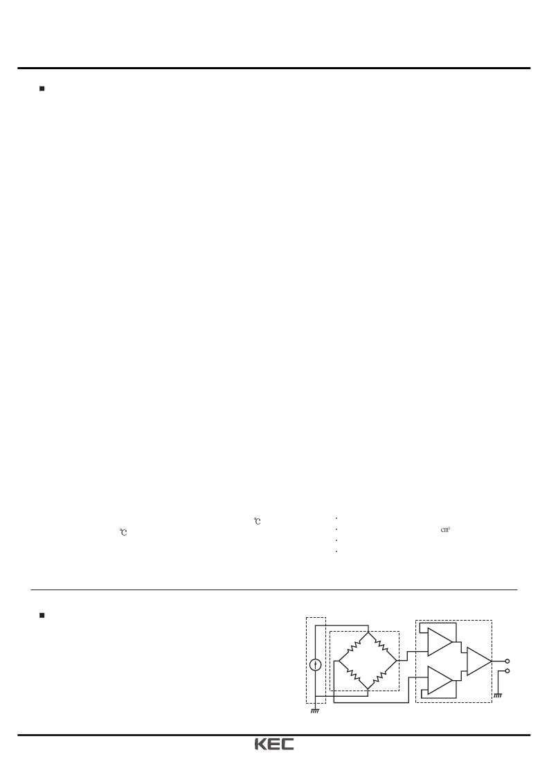
Application circuit
The Pressure sensor is designed to convert a voltage by means of
constant current drive and then, if nesessary, it amplifies the
voltage for use. The circuit shown below is a typical example of a
circuit in which the pressure sensor is used.
Pressure
Sensor
Amplifier Circuit Unit
Constant Current
Circuit Unit
OP
AMP
OP
AMP
OP
相关PDF资料 |
PDF描述 |
|---|---|
| KPF401G01 | Semiconductor Pressure Sensor |
| KPF500G01 | Semiconductor Pressure Sensor |
| KPF601G01 | Semiconductor Pressure Sensor |
| KPF801G01 | Semiconductor Pressure Sensor |
| KPF101G02 | Semiconductor Pressure Sensor |
相关代理商/技术参数 |
参数描述 |
|---|---|
| KPF201G01A | 制造商:KEC 制造商全称:KEC(Korea Electronics) 功能描述:Semiconductor Pressure Sensor |
| KPF201G02 | 制造商:KEC 制造商全称:KEC(Korea Electronics) 功能描述:Semiconductor Pressure Sensor |
| KPF201G02A | 制造商:KEC 制造商全称:KEC(Korea Electronics) 功能描述:Semiconductor Pressure Sensor |
| KPF201G03 | 制造商:KEC 制造商全称:KEC(Korea Electronics) 功能描述:Semiconductor Pressure Sensor |
| KPF201G03A | 制造商:KEC 制造商全称:KEC(Korea Electronics) 功能描述:Semiconductor Pressure Sensor |
发布紧急采购,3分钟左右您将得到回复。