- 您现在的位置:买卖IC网 > PDF目录43898 > L4972AD (STMICROELECTRONICS) 3.5 A SWITCHING REGULATOR, 200 kHz SWITCHING FREQ-MAX, PDSO20 PDF资料下载
参数资料
| 型号: | L4972AD |
| 厂商: | STMICROELECTRONICS |
| 元件分类: | 稳压器 |
| 英文描述: | 3.5 A SWITCHING REGULATOR, 200 kHz SWITCHING FREQ-MAX, PDSO20 |
| 封装: | PLASTIC, SO-20 |
| 文件页数: | 16/22页 |
| 文件大小: | 1370K |
| 代理商: | L4972AD |
3/22
L4972A
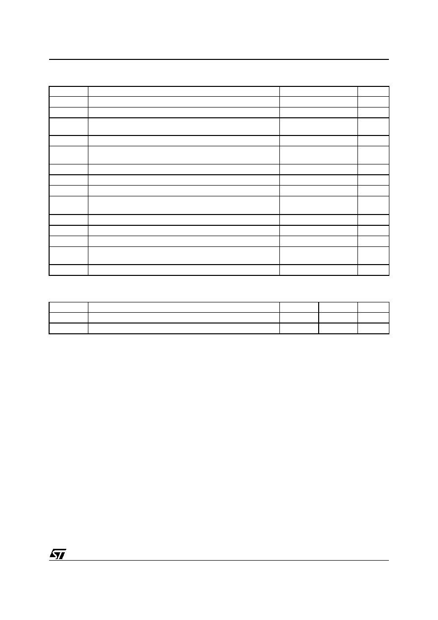
Table 3. Absolute Maximum Ratings
(*) SO-20
Table 4. Thermal Data
3
Circuit Operation
The L4972A is a 2A monolithic stepdown switching regulator working in continuous mode realized in the
new BCD Technology. This technology allows the integration of isolated vertical DMOS power transistors
plus mixed CMOS/Bipolar transistors.
The device can deliver 2A at an output voltage adjustable from 5.1V to 40V and contains diagnostic and
control functions that make it particularly suitable for microprocessor based systems.
3.1 BLOCK DIAGRAM
The block diagram shows the DMOS power transistors and the PWM control loop. Integrated functions
include a reference voltage trimmed to 5.1V ± 2%, soft start, undervoltage lockout, oscillator with feedfor-
ward control, pulse by pulse current limit, thermal shutdown and finally the reset and power fail circuit. The
reset and power fail circuit provides an output signal for a microprocessor indicating the status of the sys-
tem.
Device turn on is around 11V with a typical 1V hysterysis, this threshold porvides a correct voltage for the
driving stage of the DMOS gate and the hysterysis prevents instabilities.
An external bootstrap capacitor charge to 12V by an internal voltage reference is needed to provide cor-
rect gate drive to the power DMOS. The driving circuit is able to source and sink peak currents of around
0.5A to the gate of the DMOS transistor. A typical switching time of the current in the DMOS transistor is
50ns. Due to the fast commutation switching frequencies up to 200kHz are possible.
The PWM control loop consists of a sawtooth oscillator, error amplifier, comparator, latch and the output
Symbol
Parameter
Value
Unit
V11
Input Voltage
55
V
V11
Input Operating Voltage
50
V
V20
Output DC Voltage
Output Peak Voltage at t = 0.1
s f = 200kHz
-1
-5
V
I20
Maximum Output Current
Internally Limited
VI
Boostrap Voltage
Boostrap Operating Voltage
65
V11 + 15
V
V4, V8
Input Voltage at Pins 4, 12
12
V
V3
Reset Output Voltage
50
V
I3
Reset Output Sink Current
50
mA
V2, V7, V9,
V10
Input Voltage at Pin 2, 7, 9, 10
7
V
I2
Reset Delay Sink Current
30
mA
I7
Error Amplifier Output Sink Current
1
A
I8
Soft Start Sink Current
30
mA
Ptot
Total Power Dissipation at TPINS ≤ 90°C
at Tamb = 70°C (No copper area on PCB)
5 / 3.75(*)
1.3/1 (*)
W
TJ, Tstg
Junction and Storage Temperature
-40 to 150
°C
Symbol
Parameter
PowerDIP
SO20
Unit
Rth j-pins
Thermal Resistance Junction-Pins
max,
12
16
°C/W
Rth j-amb
Thermal Resistance Junction-ambient
max,
60
80
°C/W
相关PDF资料 |
PDF描述 |
|---|---|
| L4972AD013TR | 3.5 A SWITCHING REGULATOR, 200 kHz SWITCHING FREQ-MAX, PDSO20 |
| L4973D3.3 | 5.5 A SWITCHING REGULATOR, 300 kHz SWITCHING FREQ-MAX, PDSO20 |
| L4973V3.3 | 5.5 A SWITCHING REGULATOR, 300 kHz SWITCHING FREQ-MAX, PDIP18 |
| L4990D013TR | 1.5 A SWITCHING REGULATOR, 1000 kHz SWITCHING FREQ-MAX, PDSO16 |
| L4990 | 1.5 A SWITCHING REGULATOR, 1000 kHz SWITCHING FREQ-MAX, PDIP16 |
相关代理商/技术参数 |
参数描述 |
|---|---|
| L4972AD013TR | 功能描述:直流/直流开关调节器 5.1 to 40V 2.0 Amp RoHS:否 制造商:International Rectifier 最大输入电压:21 V 开关频率:1.5 MHz 输出电压:0.5 V to 0.86 V 输出电流:4 A 输出端数量: 最大工作温度: 安装风格:SMD/SMT 封装 / 箱体:PQFN 4 x 5 |
| L4972D | 制造商:未知厂家 制造商全称:未知厂家 功能描述:Voltage-Mode SMPS Controller |
| L4973 | 制造商:STMICROELECTRONICS 制造商全称:STMicroelectronics 功能描述:3.5A step down switching regulator |
| L4973D3 | 制造商:STMICROELECTRONICS 制造商全称:STMicroelectronics 功能描述:3.5A STEP DOWN SWITCHING REGULATOR |
| L4973D3.3 | 功能描述:直流/直流开关调节器 3.3V 3.5A Step-Down RoHS:否 制造商:International Rectifier 最大输入电压:21 V 开关频率:1.5 MHz 输出电压:0.5 V to 0.86 V 输出电流:4 A 输出端数量: 最大工作温度: 安装风格:SMD/SMT 封装 / 箱体:PQFN 4 x 5 |
发布紧急采购,3分钟左右您将得到回复。