- 您现在的位置:买卖IC网 > PDF目录30712 > L4981AD013TR (STMICROELECTRONICS) 2 A POWER FACTOR CONTROLLER, 115 kHz SWITCHING FREQ-MAX, PDSO20 PDF资料下载
参数资料
| 型号: | L4981AD013TR |
| 厂商: | STMICROELECTRONICS |
| 元件分类: | 稳压器 |
| 英文描述: | 2 A POWER FACTOR CONTROLLER, 115 kHz SWITCHING FREQ-MAX, PDSO20 |
| 封装: | SO-20 |
| 文件页数: | 10/16页 |
| 文件大小: | 2620K |
| 代理商: | L4981AD013TR |
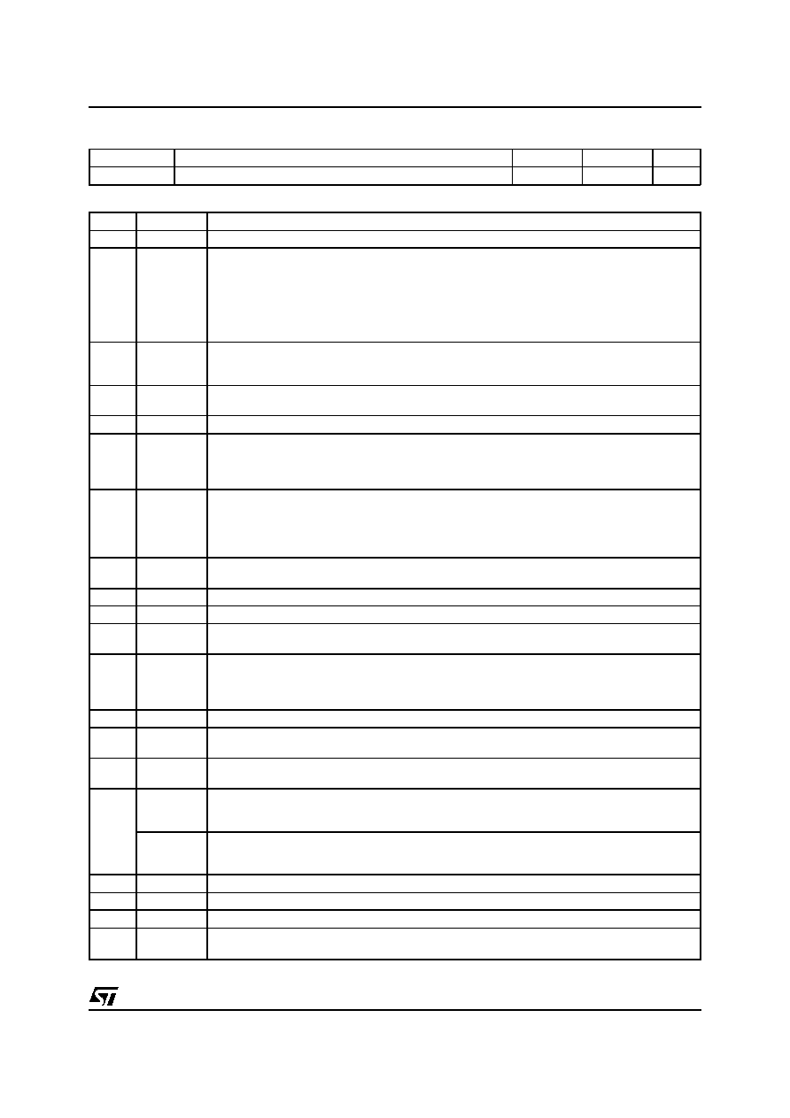
THERMAL DATA
Symbol
Parameter
DIP 20
SO 20
Unit
Rth j-amb
Thermal Resistance Junction-ambient
80
120
°C/W
PIN FUNCTIONS
N.
Name
Description
1
P-GND
Power ground.
2
IPK
L4981A peak current limiting. A current limitation is obtained using a single resistor connected
between Pin 2 and the sense resistor. To have a better precision another resistor between Pin
2 and a reference voltage (Pin 11) must be added.
L4981B peak current limiting. A precise current limitation is obtained using two external
resistor only. These resistors must be connected between the sense resistor, Pin 2 and the
reference voltage.
3
OVP
Overvoltage protection. At this input are compared an internal precise 5.1V (typ) voltage
reference with a sample of the boost output voltage obtained via a resistive voltage divider in
order to limit the maximum output peak voltage.
4
IAC
Input for the AC current. An input current proportional to the rectified mains voltage generates,
via a multiplier, the current reference for the current amplifier.
5
CA-OUT
Current amplifier output. An external RC network determinates the loop gain.
6
LFF
Load feedforward; this voltage input pin allows to modify the multiplier output current
proportionally to the load, in order to give a faster response versus load transient. The best
control is obtained working between 1.5V and 5.3V. If this function is not used, connect this pin
to the voltage reference (pin = 11).
7
VRMS
Input for proportional RMS line voltage. the VRMS input compesates the line voltage changes.
Connecting a low pass filter between the rectified line and the pin 7, a DC voltage proportional
to the input line RMS voltage is obtained. The best control is reached using input voltage
between 1.5V and 5.5V. If this function is not used connect this pin to the voltage reference
(pin = 11).
8
MULT-OUT
Multiplier output. This pin common to the multiplier output and the current amplifier N.I. input is
an high impedence input like ISENSE. The MULT-OUT pin must be taken not below -0.5V.
9ISENSE
Current amplifier inverting input. Care must be taken to avoid this pin goes down -0.5V.
10
S-GND
Signal ground.
11
VREF
Output reference voltage (typ = 5.1V).Voltage refence at
± 2% of accuracy externally available,
it’s internally current limited and can deliver an output current up to 10mA.
12
SS
A capacitor connected to ground defines the soft start time. An internal current generator
delivering 100
A (typ) charges the external capacitor defining the soft start time constant. An
internal MOS discharge, the external soft start capacitor both in overvoltage and UVLO
conditions.
13
VA-OUT
Error amplifier output, an RC network fixes the voltage loop gain characteristics.
14
VFEED
Voltage error amplifier inverting input. This feedback input is connected via a voltage divider to
the boost output voltage.
15
P-UVLO
Programmable under voltage lock out threshold input. A voltage divider between supply
voltage and GND can be connected in order to program the turn on threshold.
16
SYNC
(L4981A)
This synchronization input/output pin is CMOS logic compatible. Operating as SYNC in, a
rectangular wave must be applied at this pin. Opearting as SYNC out, a rectangular clock
pulse train is available to synchronize other devices.
FREQ-MOD
(L4981B)
Frequency modulation current input. An external resistor must be connected between pin 16
and the rectified line voltage in order to modulate the oscillator frequency. Connecting pin 16 to
ground a fixed frequency imposed by ROSC and COSC is obtained.
17
ROSC
An external resistor connected to ground fixes the constant charging current of COSC.
18
COSC
An external capacitor connected to GND fixes the switching frequency.
19
VCC
Supply input voltage.
20
GDRV
Output gate driver. Bipolar and DMOS transistors totem pole output stage can deliver peak
current in excess 1A useful to drive MOSFET or IGBT power stages.
L4981A - L4981B
3/16
相关PDF资料 |
PDF描述 |
|---|---|
| L5200-45-AH6-R | SWITCHED CAPACITOR REGULATOR, 2000 kHz SWITCHING FREQ-MAX, PDSO6 |
| L5200-50-AG6-R | SWITCHED CAPACITOR REGULATOR, 2000 kHz SWITCHING FREQ-MAX, PDSO6 |
| L5200-50-AH6-R | SWITCHED CAPACITOR REGULATOR, 2000 kHz SWITCHING FREQ-MAX, PDSO6 |
| L5201-45-AH6-R | SWITCHED CAPACITOR REGULATOR, 1300 kHz SWITCHING FREQ-MAX, PDSO6 |
| L5201L-45-AH6-R | SWITCHED CAPACITOR REGULATOR, 1300 kHz SWITCHING FREQ-MAX, PDSO6 |
相关代理商/技术参数 |
参数描述 |
|---|---|
| L4981B | 功能描述:功率因数校正 IC Very High Power RoHS:否 制造商:Fairchild Semiconductor 开关频率:300 KHz 最大功率耗散: 最大工作温度:+ 125 C 安装风格:SMD/SMT 封装 / 箱体:SOIC-8 封装:Reel |
| L4981B | 制造商:STMicroelectronics 功能描述:POWER FACTOR CORRECTOR 4981 DIP20 |
| L4981BD | 功能描述:功率因数校正 IC Very High Power RoHS:否 制造商:Fairchild Semiconductor 开关频率:300 KHz 最大功率耗散: 最大工作温度:+ 125 C 安装风格:SMD/SMT 封装 / 箱体:SOIC-8 封装:Reel |
| L4981BD | 制造商:STMicroelectronics 功能描述:POWER FACTOR CORRECTOR SMD 4981 |
| L4981BD013TR | 功能描述:功率因数校正 IC Very High Power RoHS:否 制造商:Fairchild Semiconductor 开关频率:300 KHz 最大功率耗散: 最大工作温度:+ 125 C 安装风格:SMD/SMT 封装 / 箱体:SOIC-8 封装:Reel |
发布紧急采购,3分钟左右您将得到回复。