- 您现在的位置:买卖IC网 > PDF目录43899 > L6229PDTR (STMICROELECTRONICS) BRUSHLESS DC MOTOR CONTROLLER, 2.8 A, PDSO36 PDF资料下载
参数资料
| 型号: | L6229PDTR |
| 厂商: | STMICROELECTRONICS |
| 元件分类: | 运动控制电子 |
| 英文描述: | BRUSHLESS DC MOTOR CONTROLLER, 2.8 A, PDSO36 |
| 封装: | SOP-36 |
| 文件页数: | 8/25页 |
| 文件大小: | 628K |
| 代理商: | L6229PDTR |
L6229
16/25
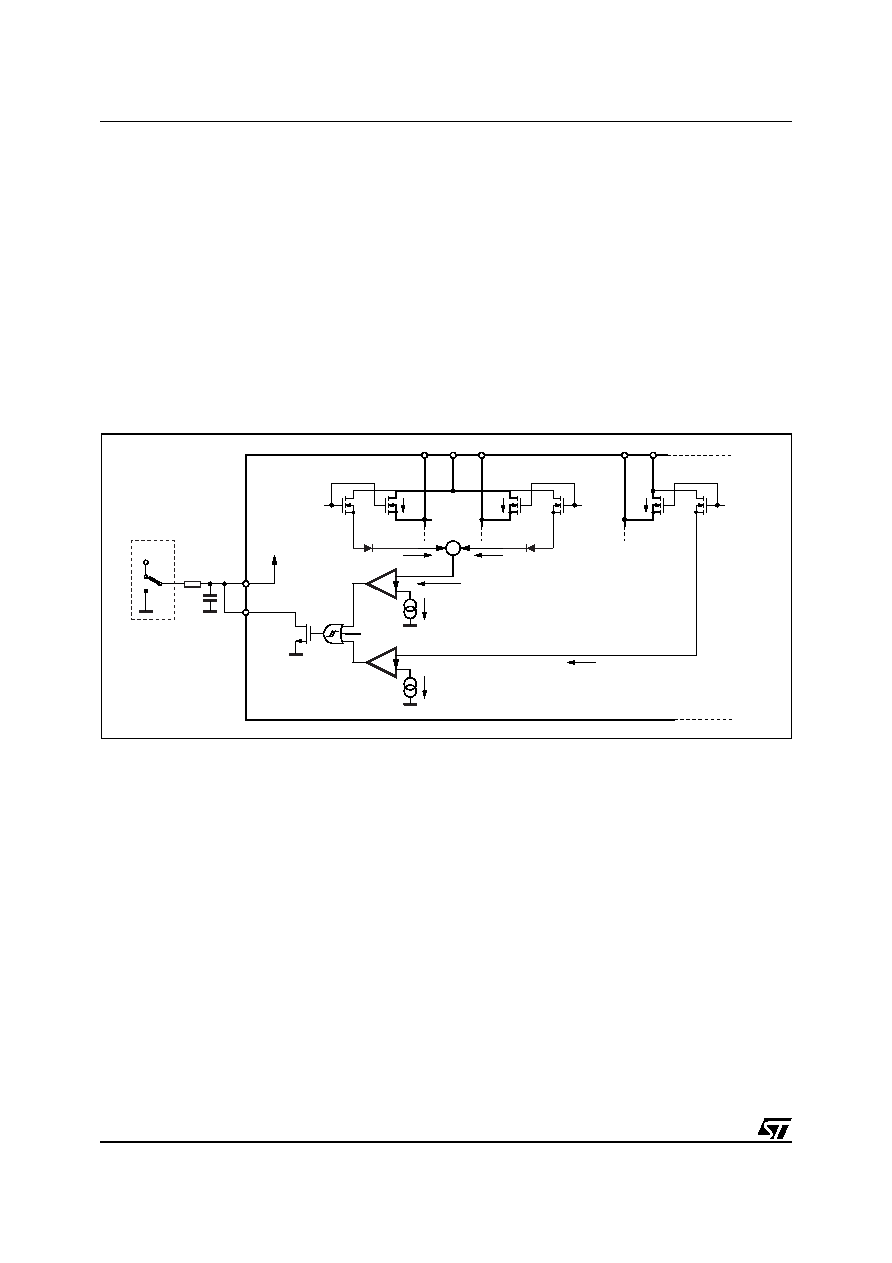
3.7 NON-DISSIPATIVE OVERCURRENT DETECTION and PROTECTION
The L6229 integrates an Overcurrent Detection Circuit (OCD) for full protection. This circuit provides Output-to-
Output and Output-to-Ground short circuit protection as well. With this internal over current detection, the exter-
nal current sense resistor normally used and its associated power dissipation are eliminated. Figure 20 shows
a simplified schematic for the overcurrent detection circuit.
To implement the over current detection, a sensing element that delivers a small but precise fraction of the out-
put current is implemented with each High Side power MOS. Since this current is a small fraction of the output
current there is very little additional power dissipation. This current is compared with an internal reference cur-
rent IREF. When the output current reaches the detection threshold (typically ISOVER = 2.8A) the OCD compar-
ator signals a fault condition. When a fault condition is detected, an internal open drain MOS with a pull down
capability of 4mA connected to pin DIAG is turned on.
The pin DIAG can be used to signal the fault condition to a
C or to shut down the Three-Phase Bridge simply
by connecting it to pin EN and adding an external R-C (see REN, CEN).
Figure 20. Overcurrent Protection Simplified Schematic
Figure 21 shows the Overcurrent Detetection operation. The Disable Time tDISABLE before recovering normal
operation can be easily programmed by means of the accurate thresholds of the logic inputs. It is affected
whether by CEN and REN values and its magnitude is reported in Figure 22. The Delay Time tDELAY before turn-
ing off the bridge when an overcurrent has been detected depends only by CEN value. Its magnitude is reported
in Figure 23
CEN is also used for providing immunity to pin EN against fast transient noises. Therefore the value of CEN
should be chosen as big as possible according to the maximum tolerable Delay Time and the REN value should
be chosen according to the desired Disable Time.
The resistor REN should be chosen in the range from 2.2K
to 180K. Recommended values for REN and CEN
are respectively 100K
and 5.6nF that allow obtaining 200s Disable Time.
+
OVER TEMPERATURE
IREF
I1+I2 / n
I1 / n
HIGH SIDE DMOS
POWER SENSE
1 cell
POWER SENSE
1 cell
POWER SENSE
1 cell
POWER DMOS
n cells
POWER DMOS
n cells
POWER DMOS
n cells
HIGH SIDE DMOS
OUT1
OUT2
VSA
OUT3
VSB
I1
I2
I3
I2/ n
I3/ n
OCD
COMPARATOR
TO GATE
LOGIC
INTERNAL
OPEN-DRAIN
RDS(ON)
40
TYP.
CEN
REN
DIAG
EN
VDD
C or LOGIC
D02IN1381
相关PDF资料 |
PDF描述 |
|---|---|
| L6235D013TR | BRUSHLESS DC MOTOR CONTROLLER, 5.6 A, PDSO24 |
| L6243D | VOICE COIL MOTOR CONTROLLER, 2.5 A, PDSO28 |
| L6245 | VOICE COIL MOTOR CONTROLLER, 1.5 A, PQFP64 |
| L6254 | DISK DRIVE MOTOR CONTROLLER, 2.1 A, PQFP44 |
| L6258E | STEPPER MOTOR CONTROLLER, 1.5 A, PDSO36 |
相关代理商/技术参数 |
参数描述 |
|---|---|
| L6229Q | 功能描述:马达/运动/点火控制器和驱动器 DMOS Driver for 3-phase DC motor RoHS:否 制造商:STMicroelectronics 产品:Stepper Motor Controllers / Drivers 类型:2 Phase Stepper Motor Driver 工作电源电压:8 V to 45 V 电源电流:0.5 mA 工作温度:- 25 C to + 125 C 安装风格:SMD/SMT 封装 / 箱体:HTSSOP-28 封装:Tube |
| L6229QTR | 功能描述:马达/运动/点火控制器和驱动器 DMOS driver 3-phrase DC motor RoHS:否 制造商:STMicroelectronics 产品:Stepper Motor Controllers / Drivers 类型:2 Phase Stepper Motor Driver 工作电源电压:8 V to 45 V 电源电流:0.5 mA 工作温度:- 25 C to + 125 C 安装风格:SMD/SMT 封装 / 箱体:HTSSOP-28 封装:Tube |
| L622C | 制造商:未知厂家 制造商全称:未知厂家 功能描述:THYRISTOR MODULE|BRIDGE|HALF-CNTLD|CA|240V V(RRM)|46A I(T) |
| L622-DBC | 制造商:未知厂家 制造商全称:未知厂家 功能描述:L series PRTDs, type L 622 DBC are designed for large volume applications where longterm stability |
| L622DY | 制造商:VCC 功能描述:LED CIRCUIT BOARD INDICATOR |
发布紧急采购,3分钟左右您将得到回复。