- 您现在的位置:买卖IC网 > PDF目录43900 > L6560AD013TR (STMICROELECTRONICS) 0.7 A POWER FACTOR CONTROLLER, PDSO8 PDF资料下载
参数资料
| 型号: | L6560AD013TR |
| 厂商: | STMICROELECTRONICS |
| 元件分类: | 稳压器 |
| 英文描述: | 0.7 A POWER FACTOR CONTROLLER, PDSO8 |
| 封装: | SO-8 |
| 文件页数: | 6/11页 |
| 文件大小: | 567K |
| 代理商: | L6560AD013TR |
OVER VOLTAGE PROTECTION OVP
The output voltage is expected to be kept by the
operation of the PFC circuits close to its reference
value that is set by the ratio of the two external re-
sistors R1 and R2 (see fig. 2), taking into consid-
eration that the non inverting input of the error
amplifier is biased inside the L6560 at 2.5V.
In steady state conditions, the current through R1
and R2 is:
ISC
=
Voutsc 2.5
R1
or ISC
=
2.5
R2
and, if the external compensation network is
made only with a capacitor C, the current through
C is equal zero.
When the output voltage increases abruptly the
current through R1 becomes:
IR1
=
Vout
2.5
R1
IR1
=
Voutsc
+ VOUT 2.5
R1
= Isc + I.
Since the current through R2 doesn’t change, the
I current must flow through the capacitor C and
enter in the error amplifier.
This current is mirrored inside the L6560, and
compared with a precise internal reference of
40
A. Whenever such 40A limit is exceed, the
OVP protection is triggered (Dynamic OVP), and
the external power transistor is switched off, until
the overvoltage situation disappears. However if
the overvoltage persists, before that the transient
condition of dynamic circuit exhausts, an internal
comparator (Static OVP) latches the OVP condi-
tion keeping the external power switch turned off
(see fig. 1).
The OVP value is threfore set by the equation
OVP =
Vout = R1 40A.
Typical values for R1, R2 and C are reported in
the application circuit. The overvoltage can be set
independently from the average output voltage.
The precision in setting the overvoltage threshold
is 7% of the overvoltage value (for instance
V =
60V
± 4.2V).
ELECTRICAL CHARACTERISTICS (continued)
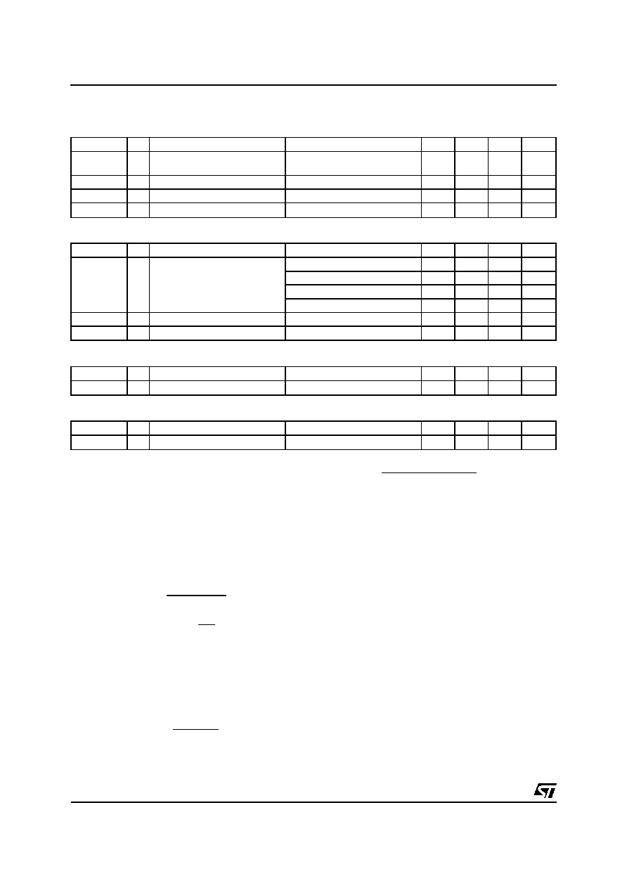
ZERO CURRENT DETECTOR
Symbol
Pin
Parameter
Test Condition
Min.
Typ.
Max.
Unit
VZCD
5
Input Threshold Voltage Rising
Edge
1.8
2.3
V
Hysteresis
0.3
0.5
0.7
V
VZCD
5
Clamp Voltage
IZCD = 3mA
5
5.7
6.4
V
VZCD
5
Clamp Voltage
IZCD = –3mA
0.4
0.7
1
V
OUTPUT SECTION
Symbol
Pin
Parameter
Test Condition
Min.
Typ.
Max.
Unit
VGD
7
Dropout Voltage
IGDsource = 200mA
1.2
2
V
IGDsource = 20mA
0.7
1
V
IGDsink = 200mA
1.5
V
IGDsink = 20mA
0.3
V
tr
7
Output Voltage Rise Time
CL = 1nF
50
120
ns
tf
7
Output Voltage Fall Time
CL = 1nF
40
100
ns
OUTPUT OVERVOLTAGE SECTION
Symbol
Pin
Parameter
Test Condition
Min.
Typ.
Max.
Unit
IOVP
2
OVP Triggering Current
36
40
44
A
RESTART TIMER
Symbol
Pin
Parameter
Test Condition
Min.
Typ.
Max.
Unit
tSTART
Start Timer
45
60
s
L6560 - L6560A
4/11
相关PDF资料 |
PDF描述 |
|---|---|
| L6560D013TR | 0.7 A POWER FACTOR CONTROLLER, PDSO8 |
| L6562ATN | SWITCHING CONTROLLER, PDIP8 |
| L6563 | 0.003 A POWER FACTOR CONTROLLER WITH POST REGULATOR, PDSO14 |
| L6563A | 0.003 A POWER FACTOR CONTROLLER WITH POST REGULATOR, PDSO14 |
| L6566BH | SWITCHING CONTROLLER, 300 kHz SWITCHING FREQ-MAX, PDSO16 |
相关代理商/技术参数 |
参数描述 |
|---|---|
| L6560D | 功能描述:开关变换器、稳压器与控制器 Wide Input Voltage RoHS:否 制造商:Texas Instruments 输出电压:1.2 V to 10 V 输出电流:300 mA 输出功率: 输入电压:3 V to 17 V 开关频率:1 MHz 工作温度范围: 安装风格:SMD/SMT 封装 / 箱体:WSON-8 封装:Reel |
| L6560D013TR | 功能描述:开关变换器、稳压器与控制器 Wide Input Voltage RoHS:否 制造商:Texas Instruments 输出电压:1.2 V to 10 V 输出电流:300 mA 输出功率: 输入电压:3 V to 17 V 开关频率:1 MHz 工作温度范围: 安装风格:SMD/SMT 封装 / 箱体:WSON-8 封装:Reel |
| L6561 | 功能描述:功率因数校正 IC Wide Input Voltage RoHS:否 制造商:Fairchild Semiconductor 开关频率:300 KHz 最大功率耗散: 最大工作温度:+ 125 C 安装风格:SMD/SMT 封装 / 箱体:SOIC-8 封装:Reel |
| L6561 | 制造商:STMicroelectronics 功能描述:PFC 90UA START + DISABLE 6561 DIP |
| L6561_04 | 制造商:STMICROELECTRONICS 制造商全称:STMicroelectronics 功能描述:POWER FACTOR CORRECTOR |
发布紧急采购,3分钟左右您将得到回复。