- 您现在的位置:买卖IC网 > PDF目录97995 > L6562DTR (STMICROELECTRONICS) 0.8 A POWER FACTOR CONTROLLER, PDSO8 PDF资料下载
参数资料
| 型号: | L6562DTR |
| 厂商: | STMICROELECTRONICS |
| 元件分类: | 稳压器 |
| 英文描述: | 0.8 A POWER FACTOR CONTROLLER, PDSO8 |
| 封装: | SO-8 |
| 文件页数: | 10/16页 |
| 文件大小: | 249K |
| 代理商: | L6562DTR |
3/16
L6562
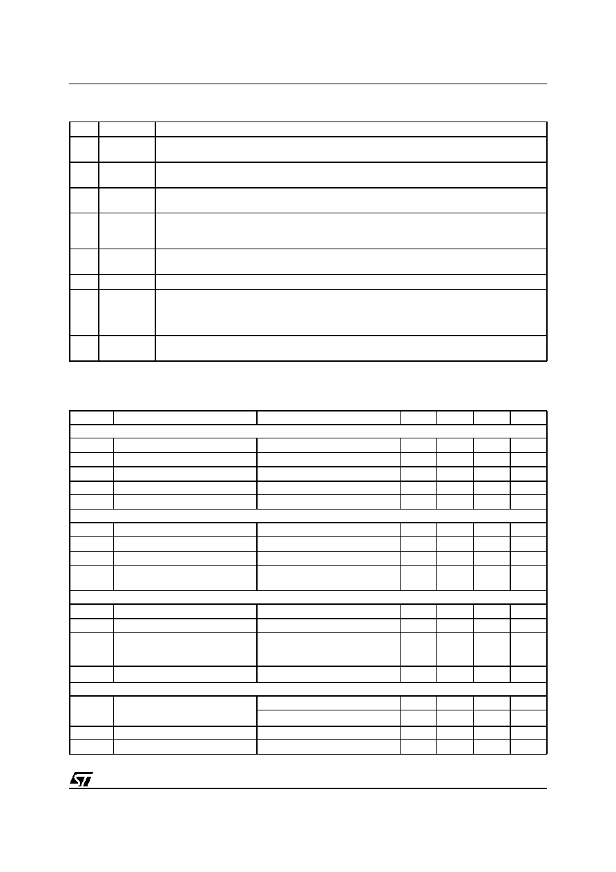
Table 4. Pin Description
N°
Pin
Function
1
INV
Inverting input of the error amplifier. The information on the output voltage of the PFC pre-
regulator is fed into the pin through a resistor divider.
2
COMP
Output of the error amplifier. A compensation network is placed between this pin and INV (pin
#1) to achieve stability of the voltage control loop and ensure high power factor and low THD.
3
MULT
Main input to the multiplier. This pin is connected to the rectified mains voltage via a resistor
divider and provides the sinusoidal reference to the current loop.
4
CS
Input to the PWM comparator. The current flowing in the MOSFET is sensed through a resistor,
the resulting voltage is applied to this pin and compared with an internal sinusoidal-shaped
reference, generated by the multiplier, to determine MOSFET’s turn-off.
5
ZCD
Boost inductor’s demagnetization sensing input for transition-mode operation. A negative-going
edge triggers MOSFET’s turn-on.
6
GND
Ground. Current return for both the signal part of the IC and the gate driver.
7
GD
Gate driver output. The totem pole output stage is able to drive power MOSFET’s and IGBT’s
with a peak current of 600 mA source and 800 mA sink. The high-level voltage of this pin is
clamped at about 12V to avoid excessive gate voltages in case the pin is supplied with a high
Vcc.
8
Vcc
Supply Voltage of both the signal part of the IC and the gate driver. The supply voltage upper
limit is extended to 22V min. to provide more headroom for supply voltage changes.
Table 5. Electrical Characteristics
(Tj = -25 to 125°C, VCC = 12, CO = 1 nF; unless otherwise specified)
Symbol
Parameter
Test Condition
Min.
Typ.
Max.
Unit
SUPPLY VOLTAGE
VCC
Operating range
After turn-on
10.3
22
V
VCCon
Turn-on threshold
(1)
11
12
13
V
VCCOff
Turn-off threshold
(1)
8.7
9.5
10.3
V
Hys
Hysteresis
2.2
2.8
V
VZ
Zener Voltage
ICC = 20 mA
22
25
28
V
SUPPLY CURRENT
Istart-up
Start-up Current
Before turn-on, VCC =11V
40
70
A
Iq
Quiescent Current
After turn-on
2.5
3.75
mA
ICC
Operating Supply Current
@ 70 kHz
3.5
5
mA
Iq
Quiescent Current
During OVP (either static or
dynamic) or VZCD =150 mV
2.2
mA
MULTIPLIER INPUT
IMULT
Input Bias Current
VVFF = 0 to 4 V
-1
A
VMULT
Linear Operation Range
0 to 3
V
Output Max. Slope
VMULT = 0 to 0.5V
VCOMP = Upper clamp
1.65
1.9
V/V
K
Gain (2)
VMULT = 1 V, VCOMP = 4 V
0.5
0.6
0.7
1/V
ERROR AMPLIFIER
VINV
Voltage Feedback Input
Threshold
Tj = 25 °C
2.465
2.5
2.535
V
10.3 V < Vcc < 22 V (1)
2.44
2.56
Line Regulation
Vcc = 10.3 V to 22V
2
5
mV
IINV
Input Bias Current
VINV = 0 to 3 V
-1
A
V
CS
V
MU L T
---------------------
相关PDF资料 |
PDF描述 |
|---|---|
| L6562D | 0.8 A POWER FACTOR CONTROLLER, PDSO8 |
| L6563HTR | POWER FACTOR CONTROLLER, PDSO16 |
| L6563H | POWER FACTOR CONTROLLER, PDSO16 |
| L6565N | 0.7 A SWITCHING CONTROLLER, PDIP8 |
| L6615N | 1-CHANNEL POWER SUPPLY SUPPORT CKT, PDIP8 |
相关代理商/技术参数 |
参数描述 |
|---|---|
| L6562DTR☞㊣☜ | 制造商:STMICROELECTRONICS 制造商全称:STMicroelectronics 功能描述:深创辉科技L6562DTR☞㊣☜现货 |
| L6562N | 功能描述:功率因数校正 IC Trans Mode PFC Cont RoHS:否 制造商:Fairchild Semiconductor 开关频率:300 KHz 最大功率耗散: 最大工作温度:+ 125 C 安装风格:SMD/SMT 封装 / 箱体:SOIC-8 封装:Reel |
| L6563 | 功能描述:功率因数校正 IC POWER SUPPLY RoHS:否 制造商:Fairchild Semiconductor 开关频率:300 KHz 最大功率耗散: 最大工作温度:+ 125 C 安装风格:SMD/SMT 封装 / 箱体:SOIC-8 封装:Reel |
| L6563_07 | 制造商:STMICROELECTRONICS 制造商全称:STMicroelectronics 功能描述:Advanced transition-mode PFC controller |
| L6563A | 功能描述:功率因数校正 IC Advanced transition mode PFC controller RoHS:否 制造商:Fairchild Semiconductor 开关频率:300 KHz 最大功率耗散: 最大工作温度:+ 125 C 安装风格:SMD/SMT 封装 / 箱体:SOIC-8 封装:Reel |
发布紧急采购,3分钟左右您将得到回复。