- 您现在的位置:买卖IC网 > PDF目录69003 > L6585DETR (STMICROELECTRONICS) POWER FACTOR CONTROLLER, PDSO20 PDF资料下载
参数资料
| 型号: | L6585DETR |
| 厂商: | STMICROELECTRONICS |
| 元件分类: | 稳压器 |
| 英文描述: | POWER FACTOR CONTROLLER, PDSO20 |
| 封装: | ROHS COMPLIANT, SOP-20 |
| 文件页数: | 8/33页 |
| 文件大小: | 2064K |
| 代理商: | L6585DETR |
第1页第2页第3页第4页第5页第6页第7页当前第8页第9页第10页第11页第12页第13页第14页第15页第16页第17页第18页第19页第20页第21页第22页第23页第24页第25页第26页第27页第28页第29页第30页第31页第32页第33页
Application information
L6585DE
16/33
The ZCD input can be connected directly to an auxiliary winding of the PFC choke in order
to turn on the MOSFET when the choke current reaches zero. This pin has internal clamps
and high current capability that makes it compliant with a very wide range of input voltage.
At startup, when PFC choke is not yet energized, an internal starter gives ZCD pulses to the
PFC gate driver with a repetition rate of approximately 15 kHz.
By turning off the MOSFET when the current reaches the threshold and turning on the
MOSFET when the choke current reaches zero, a triangular input current whose peaks are
modulated by the MULT voltage is obtained. By feeding the MULT pin with the mains
waveform, a power factor correction and THD reduction is achieved.
5.2.2
Leading edge blanking
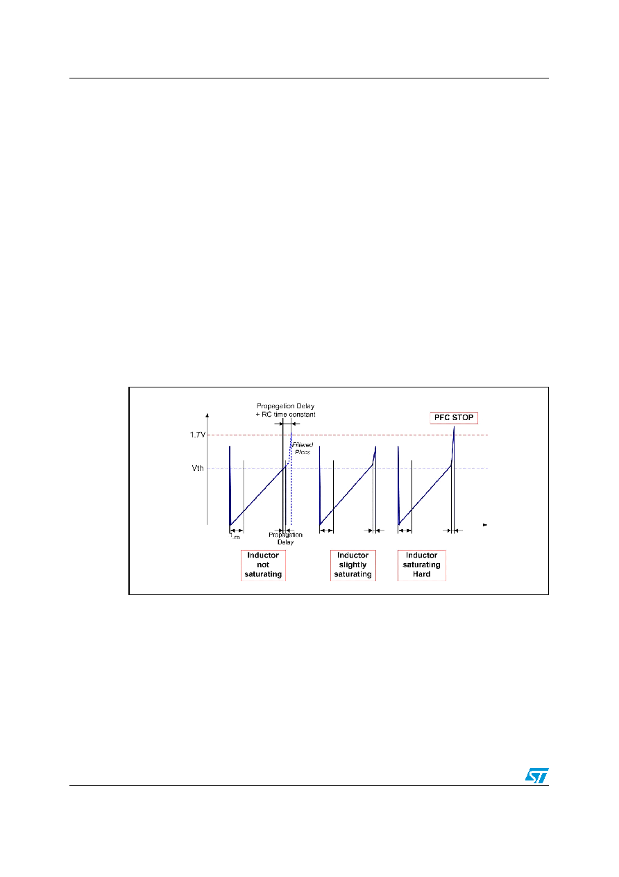
Usually current sense voltage is filtered by means of an RC network in order to avoid false
turning off of the MOSFET because of the discharge current related to parasitic drain
capacitance present at the beginning of the on time of the MOSFET. This filtering generates
a delay between the actual threshold crossing and the input triggering. During this time the
PFC inductor current increases and the choke may saturate. A leading edge blanking
structure makes the PFCCS input active only after 200 ns (typ.) after the PFG turn on. This
allows the use of inductors with lower saturation current. However, if saturation occurs, a
choke saturation protection turns off the PFC gate as soon as the voltage at pin PFCCS is
above 1.7 V.
Figure 6.
PFCCS waveforms
5.2.3
THD optimizer feature
When the input voltage passes through zero, the PFC choke cannot store energy because
of the very low voltage across it. This may cause heavy crossover distortion and subsequent
THD degradation. A small offset voltage superimposed over the MULT voltage can reduce
this issue.
The internal THD optimizer increases the performance when the mains voltage reaches
zero; this reduces crossover distortion and avoids offset introduction.
相关PDF资料 |
PDF描述 |
|---|---|
| L6598 | SWITCHING CONTROLLER, 400 kHz SWITCHING FREQ-MAX, PDIP16 |
| L6598D013TR | SWITCHING CONTROLLER, 400 kHz SWITCHING FREQ-MAX, PDSO16 |
| L6710 | 2 A SWITCHING CONTROLLER, PQFP44 |
| L6710TR | 2 A SWITCHING CONTROLLER, PQFP44 |
| L6713ATR | 2 A SWITCHING CONTROLLER, 225 kHz SWITCHING FREQ-MAX, PQFP64 |
相关代理商/技术参数 |
参数描述 |
|---|---|
| L6585DTR | 功能描述:DC/DC 开关控制器 Combo IC RoHS:否 制造商:Texas Instruments 输入电压:6 V to 100 V 开关频率: 输出电压:1.215 V to 80 V 输出电流:3.5 A 输出端数量:1 最大工作温度:+ 125 C 安装风格: 封装 / 箱体:CPAK |
| L6590 | 制造商:STMICROELECTRONICS 制造商全称:STMicroelectronics 功能描述:FULLY INTEGRATED POWER SUPPLY FIPS |
| L6590A | 制造商:未知厂家 制造商全称:未知厂家 功能描述:FULLY INTEGRATED POWER SUPPLY |
| L6590AN | 功能描述:开关变换器、稳压器与控制器 700 Volt Monolithic RoHS:否 制造商:Texas Instruments 输出电压:1.2 V to 10 V 输出电流:300 mA 输出功率: 输入电压:3 V to 17 V 开关频率:1 MHz 工作温度范围: 安装风格:SMD/SMT 封装 / 箱体:WSON-8 封装:Reel |
| L6590D | 功能描述:开关变换器、稳压器与控制器 700 Volt Monolithic RoHS:否 制造商:Texas Instruments 输出电压:1.2 V to 10 V 输出电流:300 mA 输出功率: 输入电压:3 V to 17 V 开关频率:1 MHz 工作温度范围: 安装风格:SMD/SMT 封装 / 箱体:WSON-8 封装:Reel |
发布紧急采购,3分钟左右您将得到回复。