- 您现在的位置:买卖IC网 > PDF目录79919 > L6701 (STMICROELECTRONICS) 1.5 A SWITCHING REGULATOR, 110 kHz SWITCHING FREQ-MAX, PDSO36 PDF资料下载
参数资料
| 型号: | L6701 |
| 厂商: | STMICROELECTRONICS |
| 元件分类: | 稳压器 |
| 英文描述: | 1.5 A SWITCHING REGULATOR, 110 kHz SWITCHING FREQ-MAX, PDSO36 |
| 封装: | LEAD FREE, SSO-36 |
| 文件页数: | 14/44页 |
| 文件大小: | 627K |
| 代理商: | L6701 |
第1页第2页第3页第4页第5页第6页第7页第8页第9页第10页第11页第12页第13页当前第14页第15页第16页第17页第18页第19页第20页第21页第22页第23页第24页第25页第26页第27页第28页第29页第30页第31页第32页第33页第34页第35页第36页第37页第38页第39页第40页第41页第42页第43页第44页
Obsolete
Product(s)
- Obsolete
Product(s)
L6701
10 Output Voltage Positioning
21/44
10
Output Voltage Positioning
Output voltage positioning is performed by selecting the reference DAC and by programming
from the FB pin, directly proportional to the read current, causes the output voltage to vary
according to the external RFB resistor so implementing the desired load-line resistance. The
current (IOS) sourced from the REF_IN pin causes the reference voltage to be offset according
to the resistance RFB connected.
The output voltage is then driven by the following relationship:
Both DROOP and OFFSET function can be disabled: see Section 10.1 and Section 10.3 for
details.
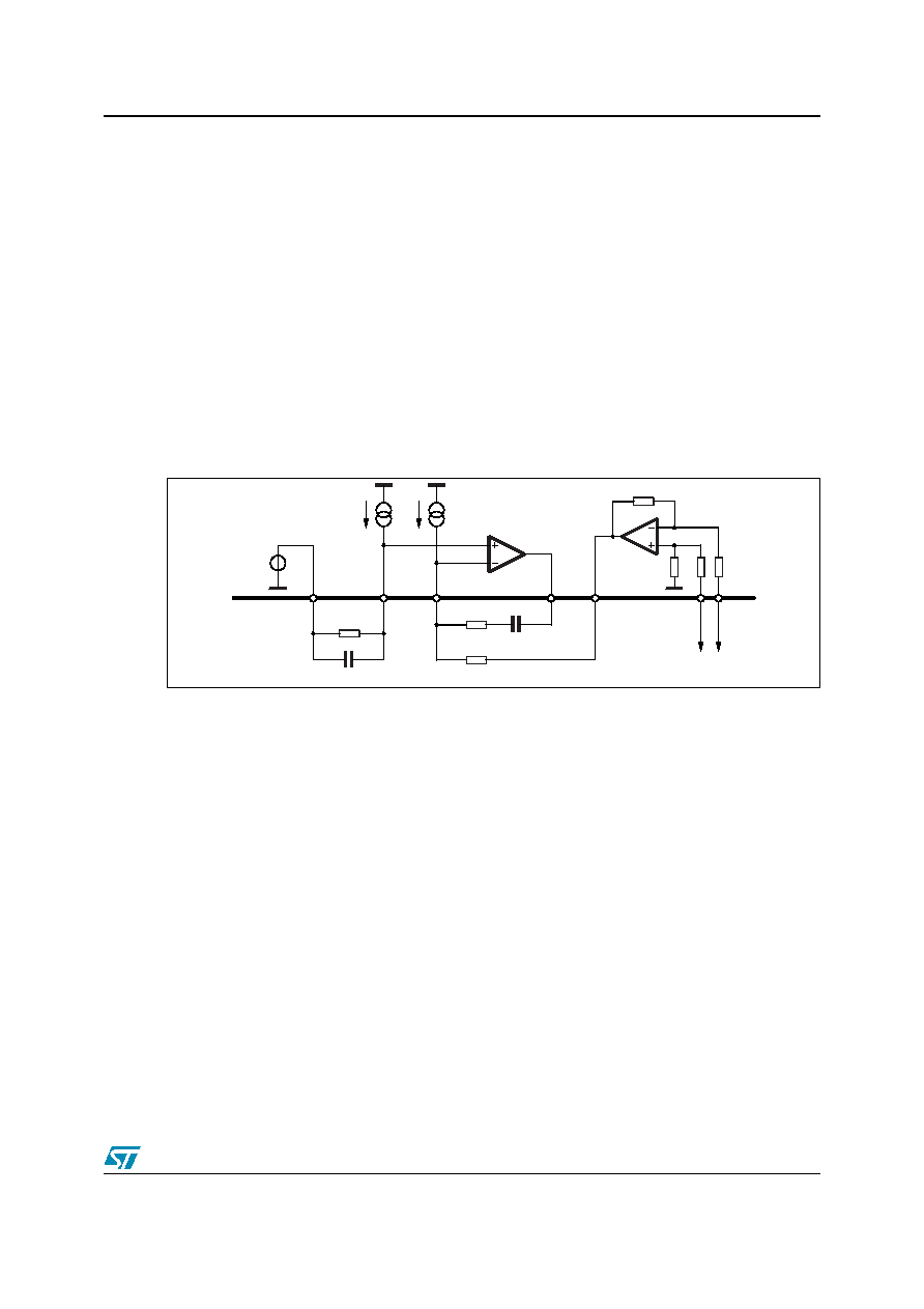
Figure 7.
Voltage Positioning
10.1
Load-Line (Droop Function - Optional)
This method "recovers" part of the drop due to the output capacitor ESR in the load transient,
introducing a dependence of the output voltage on the load current: a static error proportional to
the output current causes the output voltage to vary according to the sensed current.
Figure 8 shows the typical Current-Sense Circuit used to implement the Droop-Function in low-
cost application (saves component count). The current flowing across the three inductors is
read through the RPH - CPH filter across CS+ and CS- pins. RD programs a trans-conductance
gain and generates a current ICS proportional to the average of the currents of the three
phases. The current ICS is then mirrored and, multiplied by three, sourced by the FB pin
(IDROOP). RFB gives the final gain to program the desired load-line slope.
Considering the scheme reported on Figure 8, it is possible to observe that:
Time constant matching between the inductor (L / DCR) and the current reading filter
(
) is required to implement a real equivalent output impedance of the system so
avoiding over and/or under shoot of the output voltage as a consequence of a load transient. It
results:
V
OUT
VID
R
OS
I
OS
R
FB
I
DR O OP
–
+
=
I DR
OOP
VID
FB
COMP
VSEN
64k
FBR
FBG
64k
RF
CF
RFB
To Vcore
(Remote Sense)
REF_IN
REF_OUT
I OS
ROS
COS
I
CS
I
OUT
3
------------
1s L
DCR
+
1s R
PH
C
PH
3
+
----------------------------------------------------
DCR
R
D
-------------
=
R
PH
C
PH 3
相关PDF资料 |
PDF描述 |
|---|---|
| LP3906SQVPFP/NOPB | 2 A DUAL SWITCHING CONTROLLER, 2000 kHz SWITCHING FREQ-MAX, QCC24 |
| LS4501-7ERD3T | 1-OUTPUT 100 W AC-DC PWR FACTOR CORR MODULE |
| LS4501-7ERD8T | 1-OUTPUT 100 W AC-DC PWR FACTOR CORR MODULE |
| LT1840-7ZD | 1-OUTPUT 500 W AC-DC REG PWR SUPPLY MODULE |
| LS4001-7ERD5 | 1-OUTPUT 100 W AC-DC PWR FACTOR CORR MODULE |
相关代理商/技术参数 |
参数描述 |
|---|---|
| L6701TR | 功能描述:DC/DC 开关控制器 3 Phase Controller RoHS:否 制造商:Texas Instruments 输入电压:6 V to 100 V 开关频率: 输出电压:1.215 V to 80 V 输出电流:3.5 A 输出端数量:1 最大工作温度:+ 125 C 安装风格: 封装 / 箱体:CPAK |
| L6706 | 制造商:STMicroelectronics 功能描述:DC DC Cntrlr Single-OUT Step Down 40-Pin VFQFPN EP Tray 制造商:STMicroelectronics 功能描述:HANDHELD & COMPUTER PM - Trays 制造商:STMicroelectronics 功能描述:8-Bit VR11.1 Single CTRL w/int Driver |
| L6706TR | 功能描述:DC/DC 开关控制器 VR11.1 SINGLE PHASE CNTRL W/INT DRI RoHS:否 制造商:Texas Instruments 输入电压:6 V to 100 V 开关频率: 输出电压:1.215 V to 80 V 输出电流:3.5 A 输出端数量:1 最大工作温度:+ 125 C 安装风格: 封装 / 箱体:CPAK |
| L6709 | 功能描述:功率驱动器IC 6-Bit Dual Ph Contlr RoHS:否 制造商:Micrel 产品:MOSFET Gate Drivers 类型:Low Cost High or Low Side MOSFET Driver 上升时间: 下降时间: 电源电压-最大:30 V 电源电压-最小:2.75 V 电源电流: 最大功率耗散: 最大工作温度:+ 85 C 安装风格:SMD/SMT 封装 / 箱体:SOIC-8 封装:Tube |
| L6709TR | 功能描述:功率驱动器IC 6-Bit Dual Ph Contlr RoHS:否 制造商:Micrel 产品:MOSFET Gate Drivers 类型:Low Cost High or Low Side MOSFET Driver 上升时间: 下降时间: 电源电压-最大:30 V 电源电压-最小:2.75 V 电源电流: 最大功率耗散: 最大工作温度:+ 85 C 安装风格:SMD/SMT 封装 / 箱体:SOIC-8 封装:Tube |
发布紧急采购,3分钟左右您将得到回复。