- 您现在的位置:买卖IC网 > PDF目录97995 > L6711TR (STMICROELECTRONICS) 2 A SWITCHING CONTROLLER, 178 kHz SWITCHING FREQ-MAX, PQFP48 PDF资料下载
参数资料
| 型号: | L6711TR |
| 厂商: | STMICROELECTRONICS |
| 元件分类: | 稳压器 |
| 英文描述: | 2 A SWITCHING CONTROLLER, 178 kHz SWITCHING FREQ-MAX, PQFP48 |
| 封装: | 7 X 7 MM, 1 MM HEIGHT, TQFP-48 |
| 文件页数: | 39/50页 |
| 文件大小: | 679K |
| 代理商: | L6711TR |
第1页第2页第3页第4页第5页第6页第7页第8页第9页第10页第11页第12页第13页第14页第15页第16页第17页第18页第19页第20页第21页第22页第23页第24页第25页第26页第27页第28页第29页第30页第31页第32页第33页第34页第35页第36页第37页第38页当前第39页第40页第41页第42页第43页第44页第45页第46页第47页第48页第49页第50页
Obsolete
Product(s)
- Obsolete
Product(s)
Layout guidelines
L6711
44/50
18
Layout guidelines
Since the device manages control functions and high-current drivers, layout is one of the
most important things to consider when designing such high current applications.
A good layout solution can generate a benefit in lowering power dissipation on the power
paths, reducing radiation and a proper connection between signal and power ground can
optimize the performance of the control loops.
Integrated power drivers reduce components count and interconnections between control
functions and drivers, reducing the board space.
Here below are listed the main points to focus on when starting a new layout and rules are
suggested for a correct implementation.
18.1
Power connections.
These are the connections where switching and continuous current flows from the input
supply towards the load. The first priority when placing components has to be reserved to
this power section, minimizing the length of each connection and loop as much as possible.
To minimize noise and voltage spikes (EMI and losses) these interconnections must be a
part of a power plane and anyway realized by wide and thick copper traces: loop must be
anyway minimized. The critical components, i.e. the power transistors, must be located as
close as possible one to the other.
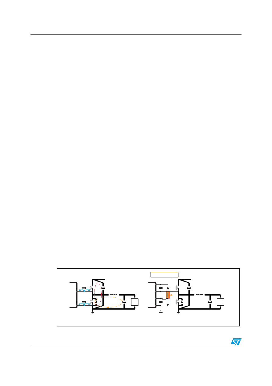
Figure 23 shows the details of the power connections involved and the current loops. The
input capacitance (CIN), or at least a portion of the total capacitance needed, has to be
placed close to the power section in order to eliminate the stray inductance generated by
the copper traces. Low ESR and ESL capacitors are preferred.
Use as much VIAs as possible when power traces have to move between different planes
on the PCB: this reduces both parasitic resistance and inductance. Moreover, reproducing
the same high-current trace on more than one PCB layer will reduce the parasitic resistance
associated to that connection.
Connect output bulk capacitor as near as possible to the load, minimizing parasitic
inductance and resistance associated to the copper trace also adding extra decoupling
capacitors along the way to the load when this results in being far from the bulk capacitor
bank.
Figure 23.
Power connections and related connections layout guidelines (same for
all phases).
L
CIN
VIN
UGATEx
PHASEx
LGATEx
PGNDx
LOAD
BOOTx
PHASEx
VCC
SGND
+Vcc
C
BOOT
L
CIN
VIN
LOAD
To limit C
BOOT
Extra-Charge
a. PCB power and ground planes areas
b. PCB small signal components placement
相关PDF资料 |
PDF描述 |
|---|---|
| L6711 | 2 A SWITCHING CONTROLLER, 178 kHz SWITCHING FREQ-MAX, PQFP48 |
| L6714TR | SWITCHING CONTROLLER, 170 kHz SWITCHING FREQ-MAX, PQFP64 |
| L6714 | SWITCHING CONTROLLER, 170 kHz SWITCHING FREQ-MAX, PQFP64 |
| L6725TR | 20 A SWITCHING CONTROLLER, 500 kHz SWITCHING FREQ-MAX, PDSO16 |
| L6728ATR | SWITCHING CONTROLLER, 660 kHz SWITCHING FREQ-MAX, PDSO10 |
相关代理商/技术参数 |
参数描述 |
|---|---|
| L6712 | 制造商:STMICROELECTRONICS 制造商全称:STMicroelectronics 功能描述:TWO-PHASE INTERLEAVED DC/DC CONTROLLER |
| L6712_05 | 制造商:STMICROELECTRONICS 制造商全称:STMicroelectronics 功能描述:TWO-PHASE INTERLEAVED DC/DC CONTROLLER |
| L6712A | 制造商:STMICROELECTRONICS 制造商全称:STMicroelectronics 功能描述:TWO-PHASE INTERLEAVED DC/DC CONTROLLER |
| L6712AD | 功能描述:开关变换器、稳压器与控制器 2-Ph Interleaved RoHS:否 制造商:Texas Instruments 输出电压:1.2 V to 10 V 输出电流:300 mA 输出功率: 输入电压:3 V to 17 V 开关频率:1 MHz 工作温度范围: 安装风格:SMD/SMT 封装 / 箱体:WSON-8 封装:Reel |
| L6712ADTR | 功能描述:开关变换器、稳压器与控制器 2-Ph Interleaved RoHS:否 制造商:Texas Instruments 输出电压:1.2 V to 10 V 输出电流:300 mA 输出功率: 输入电压:3 V to 17 V 开关频率:1 MHz 工作温度范围: 安装风格:SMD/SMT 封装 / 箱体:WSON-8 封装:Reel |
发布紧急采购,3分钟左右您将得到回复。