- 您现在的位置:买卖IC网 > PDF目录80020 > L6712AQ (STMICROELECTRONICS) 2 A SWITCHING CONTROLLER, QCC36 PDF资料下载
参数资料
| 型号: | L6712AQ |
| 厂商: | STMICROELECTRONICS |
| 元件分类: | 稳压器 |
| 英文描述: | 2 A SWITCHING CONTROLLER, QCC36 |
| 封装: | 6 X 6 MM, 1 MM HEIGHT, VFQFPN-36 |
| 文件页数: | 27/29页 |
| 文件大小: | 624K |
| 代理商: | L6712AQ |
第1页第2页第3页第4页第5页第6页第7页第8页第9页第10页第11页第12页第13页第14页第15页第16页第17页第18页第19页第20页第21页第22页第23页第24页第25页第26页当前第27页第28页第29页
7/29
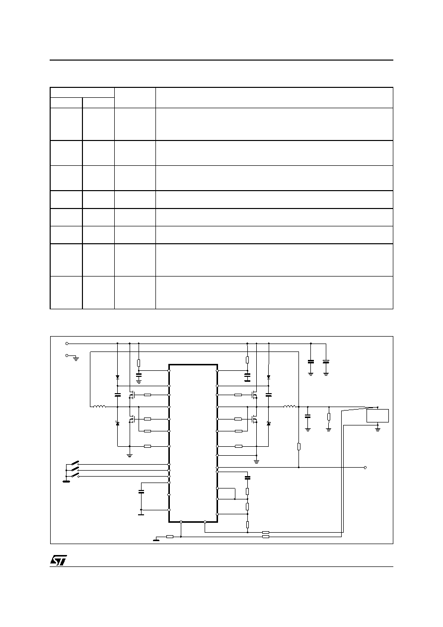
L6712A L6712
(*) Pin not reported in QFN column have to be considered as Not Connected, not internally bonded.
Figure 4. Reference Schematic
20 to 22
22 to 24
VID0-2
Voltage IDentification pins. These input are internally pulled-up. They are used to
program the output voltage as specified in Table 1 and to set the PGOOD, OVP
and UVP thresholds.
Connect to GND to program a ‘0’ while leave floating to program a ‘1’.
23
25
PGOOD
This pin is an open collector output and is pulled low if the output voltage is not
within the above specified thresholds and during soft-start.
It cannot be pulled up above 5V. If not used may be left floating.
24
27
BOOT2
Channel 2 HS driver supply. This pin supplies the relative high side driver.
Connect through a capacitor (100nF typ.) to the PHASE2 pin and through a diode
to VCC (cathode vs. boot).
25
28
UGATE2
Channel 2 HS driver output.
A little series resistor helps in reducing device-dissipated power.
26
29
PHASE2
Channel 2 HS driver return path. It must be connected to the HS2 mosfet source
and provides the return path for the HS driver of channel 2.
27
30
LGATE2
Channel 2 LS driver output.
A little series resistor helps in reducing device-dissipated power.
28
31,
32
PGND
LS drivers return path.
This pin is common to both sections and it must be connected through the
closest path to the LS mosfets source pins in order to reduce the noise injection
into the device.
PAD
THERMAL
PAD
Thermal pad connects the silicon substrate and makes a good thermal contact
with the PCB to dissipate the power necessary to drive the external
mosfets.Connect to the GND plane with several vias to improve thermal
conductivity.
Table 6. Pin Function (continued)
N. (*)
Name
Description
SO
VFQFPN
PGOOD
PGND
PGNDS2
ISEN2
LGATE2
VSEN
PHASE2
UGATE2
BOOT2
VCC
SGND
OSC / INH
VID0
VID1
VID2
REF_IN/OUT
PGNDS1
ISEN1
LGATE1
PHASE1
UGATE1
BOOT1
VCCDR
FBR
FBG
Rg
LS2
HS2
L2
C
IN
C
OUT
S1
S0
S2
Rg
LS1
L1
HS1
Vin
GNDin
PGOOD
L6712
L6712A
LOAD
Rg
FB
COMP
DROOP
R
FB
R
F
C
F
相关PDF资料 |
PDF描述 |
|---|---|
| LTC3766IUFD#PBF | SWITCHING CONTROLLER, 316 kHz SWITCHING FREQ-MAX, PQCC28 |
| L4962E/A | 3.3 A SWITCHING REGULATOR, 150 kHz SWITCHING FREQ-MAX, PZFM7 |
| LW100-01 | 4-OUTPUT 100 W AC-DC REG PWR SUPPLY MODULE |
| LS1001-7ERD7T | 1-OUTPUT 100 W AC-DC REG PWR SUPPLY MODULE |
| LT1508CN20 | POWER FACTOR CONTROLLER WITH POST REGULATOR, PDIP20 |
相关代理商/技术参数 |
参数描述 |
|---|---|
| L6712AQTR | 功能描述:开关变换器、稳压器与控制器 2-Ph Interleaved RoHS:否 制造商:Texas Instruments 输出电压:1.2 V to 10 V 输出电流:300 mA 输出功率: 输入电压:3 V to 17 V 开关频率:1 MHz 工作温度范围: 安装风格:SMD/SMT 封装 / 箱体:WSON-8 封装:Reel |
| L6712D | 功能描述:开关变换器、稳压器与控制器 2-Ph Interleaved RoHS:否 制造商:Texas Instruments 输出电压:1.2 V to 10 V 输出电流:300 mA 输出功率: 输入电压:3 V to 17 V 开关频率:1 MHz 工作温度范围: 安装风格:SMD/SMT 封装 / 箱体:WSON-8 封装:Reel |
| L6712DTR | 功能描述:开关变换器、稳压器与控制器 2-Ph Interleaved RoHS:否 制造商:Texas Instruments 输出电压:1.2 V to 10 V 输出电流:300 mA 输出功率: 输入电压:3 V to 17 V 开关频率:1 MHz 工作温度范围: 安装风格:SMD/SMT 封装 / 箱体:WSON-8 封装:Reel |
| L6712Q | 功能描述:开关变换器、稳压器与控制器 2-Ph Interleaved RoHS:否 制造商:Texas Instruments 输出电压:1.2 V to 10 V 输出电流:300 mA 输出功率: 输入电压:3 V to 17 V 开关频率:1 MHz 工作温度范围: 安装风格:SMD/SMT 封装 / 箱体:WSON-8 封装:Reel |
| L6712QTR | 功能描述:开关变换器、稳压器与控制器 2-Ph Interleaved RoHS:否 制造商:Texas Instruments 输出电压:1.2 V to 10 V 输出电流:300 mA 输出功率: 输入电压:3 V to 17 V 开关频率:1 MHz 工作温度范围: 安装风格:SMD/SMT 封装 / 箱体:WSON-8 封装:Reel |
发布紧急采购,3分钟左右您将得到回复。