- 您现在的位置:买卖IC网 > PDF目录61635 > LA2000 SPECIALTY ANALOG CIRCUIT, PSIP9 PDF资料下载
参数资料
| 型号: | LA2000 |
| 元件分类: | 模拟信号调理 |
| 英文描述: | SPECIALTY ANALOG CIRCUIT, PSIP9 |
| 封装: | SIP-9 |
| 文件页数: | 3/8页 |
| 文件大小: | 110K |
| 代理商: | LA2000 |
LA2000
No.982-3/8
1. Description of external parts
C1
Input coupling capacitor : 0.47 to 2.2μF recommended.
C2
NF capacitor : Capacitance is reduced, so the off level in input equivalent becomes lower in the bass
frequency range. We recommend 1 to 10
μF.
C3, R1
For designation of time delays : Any time delay can be obtained by adequate choice of C3 and R1. We
recommend 150k to 500k
Ω for R1.
C4, R3
Power supply ripple filter
R2
Bias resistor : For diode when pin 8 is used to drive external transistors. A 1kΩ resistor is recommen.
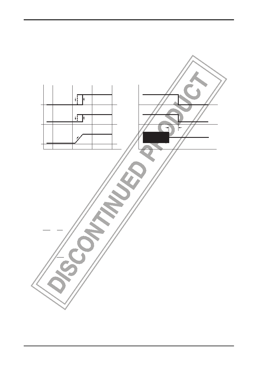
2. Individual pins and their operations
As shown above, when input level is raised and the pin 2 voltage reaches the VTH-H level of the comparator, pins 6 and
8 turn over. (VIN = -45dBm).
Pin 6 is for driving plungers, When it is on the “L” side, pin 6 turns on and can draw current up to 600mA maximum
(restricted by duty-cycle chart). It is not to be on continuously for more than 3 seconds.
Pin 7 is a diode that prevents reverse voltages induced when the plunger is turned off from on.
Pin 8 functions in phase with pin 6 and can drive external transistors (such as for MUTE ).
3. Time delays and obtaining CRs
When input signals that have been applied at a level not less than -45dBm are removed, discharging occurs through the
CR connected at pin 2, lowering pin 2 potential. A time delay is provided before the hysteresis comparator turns over.
E1
E0
= -
t
eτ
Accordingly,
t = -
τIn
E1
E0
E1/E0, within the IC, is 0.26. A desired time is obtained by an appropriate choice of
τ (τ = C3R1). Therefore, the time
delay is obtained by the following formula :
t = 1.34
× C3R1 (sec)
We recommend 150k to 500k
Ω for R when determining CR.
pin8
pin6
pin2
Gnd
pin8
pin6
VIN
Gnd
high
low
off
on
time
delay
high
low
off
VTH-H
on
-60
-50
-40
-30
VTH-L
Input signal level, VIN – dBm
E0 : Initial voltage
E1 : Threshold voltage
τ : Time constant
相关PDF资料 |
PDF描述 |
|---|---|
| LA5317M | SPECIALTY ANALOG CIRCUIT, PDSO30 |
| LA5587 | BRUSH DC MOTOR CONTROLLER, 1.4 A, PSIP5 |
| LA5587 | BRUSH DC MOTOR CONTROLLER, 1.4 A, PSIP5 |
| LA5692M | 1-CHANNEL POWER SUPPLY SUPPORT CKT, PDSO8 |
| LA5692D | 1-CHANNEL POWER SUPPLY SUPPORT CKT, PDIP8 |
相关代理商/技术参数 |
参数描述 |
|---|---|
| LA2000M | 制造商:SANYO 制造商全称:Sanyo Semicon Device 功能描述:Audio Level Sensor |
| LA2-002 DC24 | 制造商:Omron Electronic Components LLC 功能描述:REED RELAY - Japan |
| LA2002DC24 | 制造商:Omron Electronic Components LLC 功能描述:- Bulk |
| LA2-002-DC24 | 制造商:OMRON Electronic Components LLC 功能描述: 制造商:Omron Corporation 功能描述: |
| LA200P | 制造商:LEM 制造商全称:LEM 功能描述:CURRENT TRANSDUCER |
发布紧急采购,3分钟左右您将得到回复。