- 您现在的位置:买卖IC网 > PDF目录30715 > LA2335M SPECIALTY CONSUMER CIRCUIT, PDSO10 PDF资料下载
参数资料
| 型号: | LA2335M |
| 元件分类: | 消费家电 |
| 英文描述: | SPECIALTY CONSUMER CIRCUIT, PDSO10 |
| 封装: | 0.225 INCH, MFP-10 |
| 文件页数: | 2/4页 |
| 文件大小: | 65K |
| 代理商: | LA2335M |
LA2335M
No.A0305-2/4
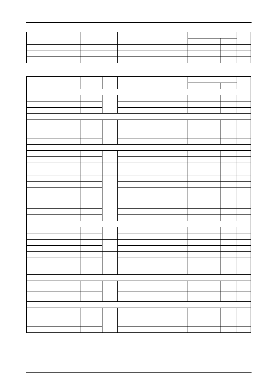
Recommended Operating Conditions at Ta = 25
°C
Ratings
Parameter
Symbol
Conditions
min
typ
max
Unit
Operating supply voltage
(VCC)
VCC op
Pin 10
4.75
5.0
5.25
V
Operating supply voltage 1 (VDD)
VDD op1
Pin4 : VDD = 3.3V
3.0
3.3
3.6
V
Operating supply voltage 2 (VDD)
VDD op2
Pin4 : VDD = 5.0V
4.75
5.0
5.25
V
Electrical Characteristics at Ta
= 25°C, VCC = 5.0V, VDD = 3.3V or 5.0V
Ratings
Parameter
Symbol
VDD
Conditions
min
typ
max
Unit
VCC current drain
With a high-level input
ICC1
TXD1 : H
4.5
6.5
9.4
mA
With a low-level input
ICC2
TXD1 : L
0.9
1.4
1.8
mA
Standby mode
ICCSTB
3.3V
/ 5.0V
STBN : L
10
A
VDD current drain
With a high-level input
IDDH1
TXD1 : H
90
150
200
A
With a low-level input
IDDL1
3.3V
TXD1 : L
200
400
600
A
With a high-level input
IDDH2
TXD1 : H
100
180
230
A
With a low-level input
IDDL2
5.0V
TXD1 : L
200
400
600
A
Transmitter
High-level input voltage
VIHDRV1
Driver differential output : 120 mV or higher
2.4
3.3
V
Low-level input voltage
VILDRV1
3.3V
Driver differential output : 20 mV or lower
0
0.5
V
High-level input voltage
VIHDRV2
Driver differential output : 120 mV or higher
3.5
5.0
V
Low-level input voltage
VILDRV2
5.0V
Driver differential output : 20 mV or lower
0
1.5
V
Bus(+) output voltage
VOHD+
TXD1 : H, TXD2 : L
1.5
3.5
V
Bus(-) output voltage
VOHD-
TXD1 : H, TXD2 : L
1.5
3.5
V
Bus(+) reference operating
voltage
VOP+
TXD1 : L, TXD2 : L
2.30
2.45
2.70
V
Bus(-) reference operating
voltage
VOP-
TXD1 : L, TXD2 : L
2.30
2.45
2.70
V
High-level output current
IHDOUT
TXD1 : H, TXD2 : L
2.7
3.8
5.0
mA
Low-level output leak current
ILDOUT
3.3V
/ 5.0V
TXD1 : L, TXD2 : L
1
A
Receiver
High-level differential input voltage
VIHR
[BUS+] - [BUS-]
65
80
120
mV
Low-level differential input voltage
VILR
3.3V
/ 5.0V
[BUS+] - [BUS-]
20
40
60
mV
High-level output voltage
VOHR1
Load : 47k
// 18pF
2.4
3.3
V
Low-level output voltage
VOLR1
3.3V
Load : 47k
// 18pF
0
0.5
V
High-level output voltage
VOHR2
Load : 47k
// 18pF
4.0
5.0
V
Low-level output voltage
VOLR2
5.0V
Load : 47k
// 18pF
0
1.0
V
Input hysteresis voltage
VIHYS
3.3V
/ 5.0V
VIHR - VILR
20
40
60
mV
Total delay time (See note.)
L
→H
TTDR
Compared at the 90% values of the TXD and
RXD amplitudes
500
800
ns
H
→L
TTDF
3.3V
/ 5.0V
Compared at the 10% values of the TXD and
RXD amplitudes
500
800
ns
Standby
On
VILSTB1
0
0.5
V
Off
VIHSTB1
3.3V
2.4
3.3
V
On
VILSTB2
0
1.0
V
Off
VIHSTB2
5.0V
3.5
5.0
V
Note : The characteristics when a load of RL = 47k and a capacitance of 18pF is connected to pin 3.
相关PDF资料 |
PDF描述 |
|---|---|
| LA2335M | SPECIALTY CONSUMER CIRCUIT, PDSO10 |
| LA2610 | SPECIALTY CONSUMER CIRCUIT, PSIP12 |
| LA2615M | SPECIALTY CONSUMER CIRCUIT, PDSO16 |
| LA2615 | SPECIALTY CONSUMER CIRCUIT, PDIP16 |
| LA2616V | SPECIALTY CONSUMER CIRCUIT, PDSO16 |
相关代理商/技术参数 |
参数描述 |
|---|---|
| LA2340 | 制造商:LIGITEK 制造商全称:LIGITEK electronics co., ltd. 功能描述:ROUND TYPE LED LAMPS |
| LA2341-41 | 制造商:未知厂家 制造商全称:未知厂家 功能描述: |
| LA2341-42B | 制造商:未知厂家 制造商全称:未知厂家 功能描述: |
| LA2341R41 | 制造商:未知厂家 制造商全称:未知厂家 功能描述:Optoelectronic |
| LA2341R42B | 制造商:未知厂家 制造商全称:未知厂家 功能描述: |
发布紧急采购,3分钟左右您将得到回复。