- 您现在的位置:买卖IC网 > PDF目录32287 > LA3607 1 CHANNEL(S), EQUALIZER CIRCUIT, PDIP20 PDF资料下载
参数资料
| 型号: | LA3607 |
| 元件分类: | 音频控制 |
| 英文描述: | 1 CHANNEL(S), EQUALIZER CIRCUIT, PDIP20 |
| 封装: | 0.300 INCH, DIP-20 |
| 文件页数: | 5/7页 |
| 文件大小: | 101K |
| 代理商: | LA3607 |
LA3607
No.2277-5/7
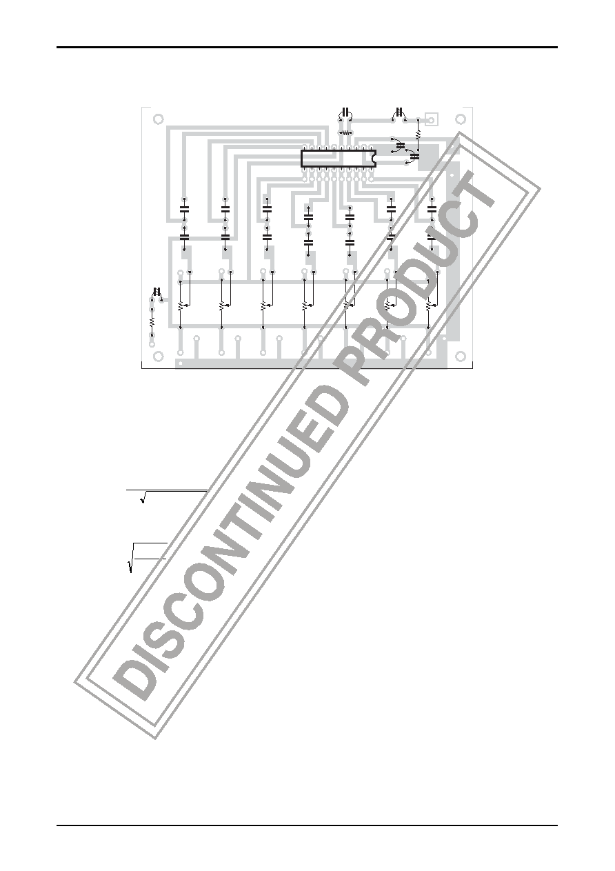
Sample Printed Circuit Pattern (Cu-foilde side)
120
× 95mm2
bottom view
+
8.2k
Ω
8.2k
Ω
VR
100kB
×7
10k
Ω
3.3
μF/16V
3.3
μF/16V
47
μF/15V
22
μF/16V
0.07
μF
1.25
μF
0.028
μF
0.5
μF
0.01
μF
0.19
μF
0.004
μF
0.075
μF
1600pF
0.03
μF
280pF
0.005
μF
690pF
0.0125
μF
LA3607
11
20
10
1
470pF
fo (resonance frequency)
In the sample application circuit, fo for each of 7 bands is set as follows :
fo = 60Hz, 150Hz, 400Hz, 1kHz, 2.5kHz, 6kHz, 15kHz
fo is calculated using the following formula.
Q (quality factor)
Q is calculated using the following formula.
When Q is increased, the frequency band affected by the resonance circuit is narrowed and a clear distinction
between this band and adjacent band is provided, but the frequency response swells greatly at all boost mode and
the peak of the composite frequency is lowered. The above must be considered to fix C1, C2.
Description of external parts
C1, C2 : Capacitors used to fix fo (resonance frequency)
C3
: Input capacitor. Decreasing the capacitor value lowers the frequency response at low frequencies.
C4
: Decoupling capacitor. Decreasing the capacitor value makes the effect of power supply stronger, whereby
repple is liable to occur.
C5
: Power capacitor.
C6
: Putput capacitor. Decreasing the capacitor value lowers the frequency response at low frequencies.
Proper cares in using IC
Maximum supply voltage VCC max 20V must not be exceeded. The operating voltage is in the range of 5 to 15V.
Application of power with the pin-to-pin spaces shorted causes breakdown or deterioration of the IC to occur.
When mounting the IC on the board of applying power, make sure that the pin-to-pin spaces are not shorted with
solder, etc.
2
R
1
R
2
C
1
C
2
1
fo
=
π
1
R
2
C
2
R
1
C
Q
=
相关PDF资料 |
PDF描述 |
|---|---|
| LA4146 | 0.9 W, 1 CHANNEL, AUDIO AMPLIFIER, PSIP9 |
| LA42031 | 5 W, 1 CHANNEL, AUDIO AMPLIFIER, SFM13 |
| LA42031 | 5 W, 1 CHANNEL, AUDIO AMPLIFIER, SFM13 |
| LA42152 | 15 W, 2 CHANNEL, AUDIO AMPLIFIER, SFM12 |
| LA4262 | 7 W, 2 CHANNEL, AUDIO AMPLIFIER, SFM10 |
相关代理商/技术参数 |
参数描述 |
|---|---|
| LA360R | 制造商:未知厂家 制造商全称:未知厂家 功能描述:Optoelectronic |
| LA3610 | 制造商:未知厂家 制造商全称:未知厂家 功能描述: |
| LA3610M | 制造商:未知厂家 制造商全称:未知厂家 功能描述: |
| LA36125 | 制造商:Schneider Electric 功能描述:MOLDED CASE CIRCUIT BREAKER 600V 125A |
| LA36150 | 制造商:Schneider Electric 功能描述:MOLDED CASE CIRCUIT BREAKER 600V 150A |
发布紧急采购,3分钟左右您将得到回复。