- 您现在的位置:买卖IC网 > PDF目录61635 > LA6565 (SANYO SEMICONDUCTOR CO LTD) BRUSH DC MOTOR CONTROLLER, 1 A, PDSO36 PDF资料下载
参数资料
| 型号: | LA6565 |
| 厂商: | SANYO SEMICONDUCTOR CO LTD |
| 元件分类: | 运动控制电子 |
| 英文描述: | BRUSH DC MOTOR CONTROLLER, 1 A, PDSO36 |
| 封装: | 0.375 INCH, HSOP-36 |
| 文件页数: | 2/5页 |
| 文件大小: | 116K |
| 代理商: | LA6565 |
LA6565
No.7817-2/8
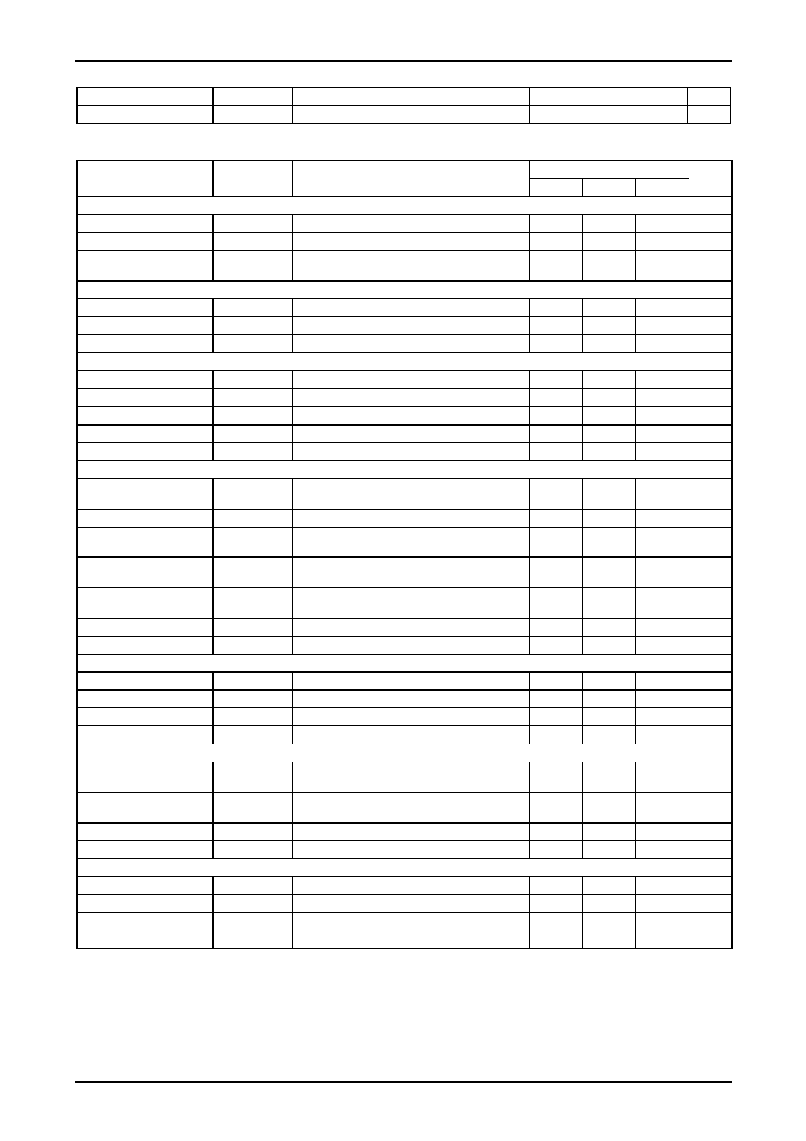
Recommended Operating Conditions at Ta = 25
°C
Parameter
Symbol
Conditions
Ratings
Unit
Supply voltage
VCC
5.6 to 13
V
Electrical Characteristics at Ta
= 25°C, VCC1 = VCC2 = 8V, VREF = 2.5V
Ratings
Parameter
Symbol
Conditions
min
typ
max
Unit
Overall
Quiescent current when o
ICC-ON
BTL amplifier output on, loading block off *1
30
50
mA
Quiescent current when off
ICC-OFF
All outputs off *1
10
15
mA
Thermal shutdown circuit
operating temperature
TSD
*7
150
175
200
°C
VREF Amplifier
VREF amplifier offset voltage
VREF-OFFSET
-10
+10
mV
VREF input voltage range
VREF-IN
1
VCC-1.5
V
VREF-OUT output current
I-VREF-OUT
1
mA
Operational Amplifier (Independent)
Input voltage range
VIN(OP)
0
VCC-1.5
V
Output current (sink)
SINK(OP)
2
mA
Output current (source)
SOURCE(OP)
300
500
A
Output offset voltage
VOFF(OP)
-10
+10
mV
Residual current (sink)
VCE-SINK(OP)
IO(sink side) = 1mA
0.6
V
BTL Amplifier Block (Channels 1 to 4)
Output offset voltage
VOFF
The voltage difference between each channel
outputs *2, *3
-50
+50
mV
Input voltage range
VIN
Input voltage range of the input operational amplifiers
0
VCC-1.5
V
Output voltage
VO
IO = 0.5A, the voltage between VO+ and VO- in each
channel
5.7
6.2
V
Closed circuit voltage gain
VG
The gain from the input to the output with the input
amplifier set to 0dB*2, *3
7.2
8
9
times
Slew rate SR
SR
For the independent amplifier. Times 2 when
between outputs.*7
0.5
V/
s
Muting on voltage
VMUTE-ON
The output on voltage, for each mute function *4
2.5
V
Muting off voltage
VMUTE-OFF
The output off voltage, for each mute function *4
0.5
V
Input Amplifier Block (Channels 1 and 2)
Input voltage range
VIN-OP
0
VCC-1.5
V
Output current (sink)
SINK-OP
2
mA
Output current (source)
SOURCE-OP
*5
300
500
A
Output offset voltage
VOFF-OP
-10
+10
mV
Loading Block (Channel 5, H bridge circuit)
Output voltage
VO-LOAD
For forward/reverse operation, IO = 0.5A,
VCONT = VCC*
5.7
6.5
V
Braking output saturation
voltage
VCE-BREAK
The output voltage during braking *6
0.3
V
Low-level input voltage
VIN-L
1
V
High-level input voltage
VIN-H
2
V
Power Supply Block (Uses an external 2SB632K PNP-transistor)
Power supply output
VOUT
IO = 200mA
1.260
1.285
1.310
V
REG-IN sink current
REG-IN-SINK
External PNP-transistor base current
5
10
mA
Line regulation
VOLN
6V
≤ VCC ≤ 12V, IO = 200mA
10
100
mV
Load regulation
VOLD
5mA
≤ IO ≤ 200mA
10
100
mV
*1: The total current dissipation for VCCP1, VCCP2, and VCCS with no load.
*2: The input amplifier is a buffer amplifier.
*3: The voltage difference between the two sides of the load (12
).
*4: When the MUTE pin is high, the output will be on, and when low, the output will be off (high-impedance state).
*5: The input operational amplifier source is constant current. Since the 11k
resistor between this and the next stage functions as the load, the input
operational amplifier gain must be set carefully.
*6: The braking operation is a short (to ground) braking operation. The sink side output is on at this time.
*7: Design guarantee.
相关PDF资料 |
PDF描述 |
|---|---|
| LA6565 | BRUSH DC MOTOR CONTROLLER, 1 A, PDSO36 |
| LA6584 | BRUSHLESS DC MOTOR CONTROLLER, 1.2 A, PDSO14 |
| LA6584 | BRUSHLESS DC MOTOR CONTROLLER, 1.2 A, PDSO14 |
| LA7954 | 4-CHANNEL, AUDIO/VIDEO SWITCH, SIP9 |
| LA7957 | DUAL 3-CHANNEL, AUDIO/VIDEO SWITCH, PDIP20 |
相关代理商/技术参数 |
参数描述 |
|---|---|
| LA6565_09 | 制造商:SANYO 制造商全称:Sanyo Semicon Device 功能描述:For CD and DVD players 5-channel Driver (BTL:4ch,H-bridge:1ch) |
| LA6565-A-TE-L-E | 制造商:ON Semiconductor 功能描述:MOTOR DRIVER - Tape and Reel 制造商:ON Semiconductor 功能描述:REEL / MOTOR DRIVER |
| LA6565-TE-L-E | 功能描述:功率驱动器IC MOTOR DRIVER RoHS:否 制造商:Micrel 产品:MOSFET Gate Drivers 类型:Low Cost High or Low Side MOSFET Driver 上升时间: 下降时间: 电源电压-最大:30 V 电源电压-最小:2.75 V 电源电流: 最大功率耗散: 最大工作温度:+ 85 C 安装风格:SMD/SMT 封装 / 箱体:SOIC-8 封装:Tube |
| LA6565VR | 制造商:SANYO 制造商全称:Sanyo Semicon Device 功能描述:Monolithic Linear IC Five-Channel CD Actuator Driver (BTL: 4 channels, H bridge: 1 channel) |
| LA6565VR-TLM-E | 制造商:ON Semiconductor 功能描述:MOTOR DRIVER - Tape and Reel 制造商:Rochester Electronics LLC 功能描述: 制造商:ON Semiconductor 功能描述:REEL / MOTOR DRIVER 制造商:Sony Semiconductor Solutions Division 功能描述: |
发布紧急采购,3分钟左右您将得到回复。