- 您现在的位置:买卖IC网 > PDF目录30720 > LA70020M 6 CHANNEL, VIDEO PREAMPLIFIER, PDSO36 PDF资料下载
参数资料
| 型号: | LA70020M |
| 元件分类: | 音频/视频放大 |
| 英文描述: | 6 CHANNEL, VIDEO PREAMPLIFIER, PDSO36 |
| 封装: | MFP-36 |
| 文件页数: | 6/13页 |
| 文件大小: | 215K |
| 代理商: | LA70020M |
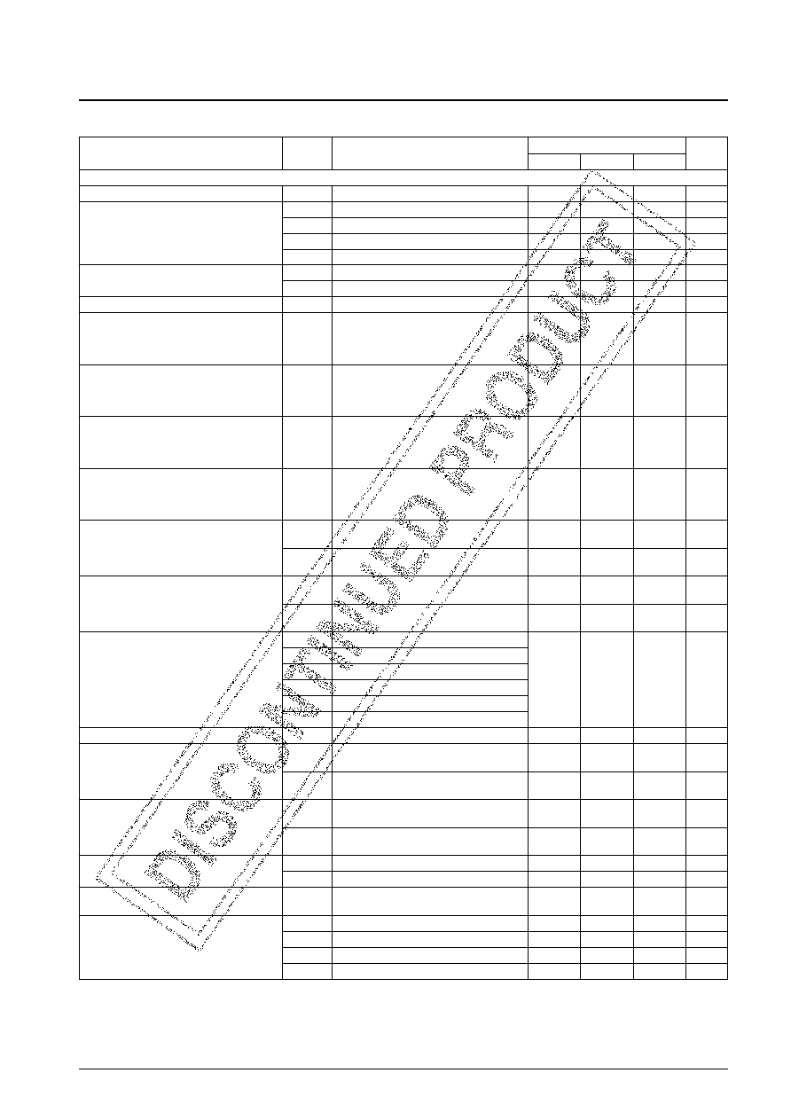
No. 5711-2/13
LA70020, 70020M
Parameter
Symbol
Conditions
Ratings
Unit
min
typ
max
Playback Mode
Current drain
ICCP
Current flowing into pin 13
44
53
60
mA
SP-L CH1
GVP1VIN = 38 mVp-p, f = 4 MHz
56
59
62
dB
Voltage gain
SP-H CH2
GVP256
59
62
dB
EP-L CH3
GVP356
59
62
dB
EP-H CH4
GVP456
59
62
dB
Voltage gain difference
GVP1GVP1 — GVP2
–10
+1
dB
GVP2GVP3 — GVP4
–10
+1
dB
Intermode gain difference
GVP3GVP3 — GVP1
–10
+1
dB
CH1
VNIN1
Ratio of the output from a 1.1 MHz low pass
Converted input noise voltage
CH2
VNIN2
filter to the output with no input under the
1.0
1.5
Vrms
CH3
VNIN3
same conditions as those used for measuring
CH4
VNIN4
voltage gain.
CH1
Vfp1
Ratios of the output for VIN = 38 mVp-p and
Frequency characteristic
CH2
Vfp2
f = 7 MHz to the voltage gains GVP1, GVP2,
–2.5
0
dB
CH3
Vfp3
GVP3, and GVP4.
CH4
Vfp4
CH1
VHDP1 Ratio of the 8 MHz (secondary) component of
Secondary harmonic distortion
CH2
VHDP2 the output to its 4 MHz (primary) component
–40
–35
dB
CH3
VHDP3 for VIN = 38 mVp-p and f = 4 MHz.
CH4
VHDP4
CH1
VOMP1 Output level, for f = 1 MHz, at which the ratio
Maximum output level
CH2
VOMP2 of the 3 MHz (tertiary) component to the
1.0
1.2
Vp-p
CH3
VOMP3 1 MHz (primary) component is -30 dB.
CH4
VOMP4
VCR1
Ratio of the output for VIN = 38 mVp-p and
–40
–35
dB
Crosstalk SP
f = 4 MHz to GVP1.
VCR2
Ratio of the output for VIN = 38 mVp-p and
–40
–35
dB
f = 4 MHz to GVP2.
VCR3
Ratio of the output for VIN = 38 mVp-p and
–40
–35
dB
Crosstalk EP
f = 4 MHz to GVP3.
VCR4
Ratio of the output for VIN = 38 mVp-p and
–40
–35
dB
f = 4 MHz to GVP4.
VODC1 CH1 — CH2
VODC2 CH3 — CH4
Output DC offset
VODC3 CH1 — CH3
–100
0
+100
mV
VODC4 CH2 — CH4
VODC5 CH1 — CH4
VODC6 CH2 — CH3
Envelope detector output pin voltage
VENV
T12 DC level with no signal input.
0
0.8
1.4
V
VENVSP1
T12 DC level at which T13A output level is
2.0
2.5
3.0
V
Envelope detector output pin voltage SP
150 mVp-p for f = 4 MHz.
VENVSP2
T12 DC level at which T13A output level is
4.0
4.5
5.0
V
400 mVp-p for f = 4 MHz.
VENVEP1
T12 DC level at which T13A output level is
2.0
2.5
3.0
V
Envelope detector output pin voltage EP
125 mVp-p for f = 4 MHz.
VENVEP2
T6 DC level at which T7A output level is
4.0
4.5
5.0
V
300 mVp-p for f = 4 MHz.
Comparator output voltage
VCOMP1
T8 DC level for VIN = 38 mVp-p and f = 4 MHz.
0.4
0.7
V
VCOMP2
T8 DC level for VIN = 38 mVp-p and f = 4 MHz.
4.5
4.8
V
SW-Tr on resistance during playback
RPON24
DC difference for 1 and 2 mA current inputs.
4
6
RPON29
TR1-1
Normal
→ Trick1 : *1
3.2
5.0
V
Trick threshold level
TR1-2
Trick1
→ Normal
1.2
2.8
V
TR2-1
Normal
→ Trick2 : *1
0.0
0.8
V
TR2-2
Trick2
→ Normal
1.2
2.8
V
Electrical Characteristics at Ta = 25°C (Video Circuits)
Continued on next page.
相关PDF资料 |
PDF描述 |
|---|---|
| LA70020 | 6 CHANNEL, VIDEO PREAMPLIFIER, PDIP36 |
| LA70050W | 3 CHANNEL, VIDEO PREAMPLIFIER, PQFP48 |
| LA7051 | SPECIALTY CONSUMER CIRCUIT, PSIP9 |
| LA7053 | SPECIALTY CONSUMER CIRCUIT, PSIP9 |
| LA7054Z | SPECIALTY CONSUMER CIRCUIT, PZIP9 |
相关代理商/技术参数 |
参数描述 |
|---|---|
| LA7003 | 制造商:未知厂家 制造商全称:未知厂家 功能描述: |
| LA7003S | 制造商:未知厂家 制造商全称:未知厂家 功能描述: |
| LA7005 | 制造商:未知厂家 制造商全称:未知厂家 功能描述: |
| LA70056T-MPB-E | 制造商:ON Semiconductor 功能描述:HEAD AMPLIFIER FOR DVC |
| LA7005S | 制造商:未知厂家 制造商全称:未知厂家 功能描述: |
发布紧急采购,3分钟左右您将得到回复。