- 您现在的位置:买卖IC网 > PDF目录30721 > LA72670BM SPECIALTY CONSUMER CIRCUIT, PQFP80 PDF资料下载
参数资料
| 型号: | LA72670BM |
| 元件分类: | 消费家电 |
| 英文描述: | SPECIALTY CONSUMER CIRCUIT, PQFP80 |
| 封装: | 14 X 14 MM, QFP-80 |
| 文件页数: | 7/11页 |
| 文件大小: | 332K |
| 代理商: | LA72670BM |
LC89057W-VF4A-E
No.7202-5/59
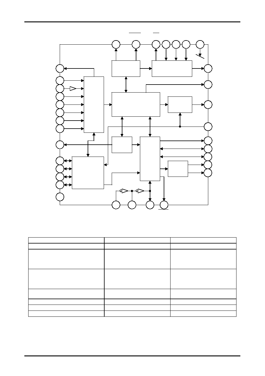
6. Block Diagram
7. Comparison between LC89057W-VF4 and LC89057W-VF4A
Table 7.1 Difference between LC89057W-VF4 and LC89057W-VF4A
Item
LC89057W-VF4
LC89057W-VF4A
DIR function: External synchronization mode
256fs clock input
256fs or 512fs clock input
DIR function: Setting of RERR wait time after PLL
is locked
After preamble B is counted 6.
After preamble B is counted 12.
After preamble B is counted 24.
After preamble B is counted 48.
After preamble B is counted 3.
After preamble B is counted 6.
After preamble B is counted 12.
After preamble B is counted 24.
DIR function: Setting of clock wait time after PLL is
unlocked
50
μs from when oscillation amplifier starts
100
μs from when oscillation amplifier starts
200
μs from when oscillation amplifier starts
400
μs from when oscillation amplifier starts
0
μs from when oscillation amplifier starts
50
μs from when oscillation amplifier starts
100
μs from when oscillation amplifier starts
200
μs from when oscillation amplifier starts
DIR function: Channel status bit output
Microcontroller read out
Microcontroller read out or terminal output
(full decode processing possible)
DIR function: Preamble B info output
×
DIT function: System clock
256fs clock input
256fs or 128fs clock input
DIT function: Preamble B info output
×
32
33
35
48
39
38
41
Cbit, Ubit
Microcontroller
I/F
37
EMPHA/UO/CO
AUDIO/VO
INT
CL
CE
CI
XMODE
Demodulation
&
Lock detect
Data
Selector
21
36
DO
RERR
RDATA
PLL
Clock
Selector
Input
Selector
2
3
4
5
8
9
10
13
Modulation
or
Parallel Port
RX0
RX1
RX2
RX3
RX4
RX5/VI
RX6/UI
LPF
44
TMCK/PIO0
45
TBCK/PIO1
46
TLRCK/PIO2
47
TDATA/PIO3
48
TXO/PIOEN
24
SDIN
16
RMCK
17
RBCK
20
RLRCK
22
SBCK
23
SLRCK
1/N
27
1
RXOUT
29
28
34
XIN
XOUT
XMCK
CKST/PB
相关PDF资料 |
PDF描述 |
|---|---|
| LA72670BM | SPECIALTY CONSUMER CIRCUIT, PQFP80 |
| LA72670M | SPECIALTY CONSUMER CIRCUIT, PQFP80 |
| LA72680M | SPECIALTY CONSUMER CIRCUIT, PQFP80 |
| LA72680M | SPECIALTY CONSUMER CIRCUIT, PQFP80 |
| LA72700V | SPECIALTY CONSUMER CIRCUIT, PDSO36 |
相关代理商/技术参数 |
参数描述 |
|---|---|
| LA72670BM-MPB-E | 制造商:ON Semiconductor 功能描述: |
| LA72680M | 制造商:SANYO 制造商全称:Sanyo Semicon Device 功能描述:JAPAN TV Sound Multiplex Demodulation HiFi Sound Signal Processor |
| LA72680M-MPB-E | 制造商:ON Semiconductor 功能描述: 制造商:Sony Semiconductor Solutions Division 功能描述: |
| LA7270 | 制造商:SANYO 制造商全称:Sanyo Semicon Device 功能描述:VHS VTR Playback Head Amplifier Recording Amplifier |
| LA72700 | 制造商:Contact Us 功能描述: |
发布紧急采购,3分钟左右您将得到回复。