- 您现在的位置:买卖IC网 > PDF目录30721 > LA72700V (SANYO SEMICONDUCTOR CO LTD) SPECIALTY CONSUMER CIRCUIT, PDSO36 PDF资料下载
参数资料
| 型号: | LA72700V |
| 厂商: | SANYO SEMICONDUCTOR CO LTD |
| 元件分类: | 消费家电 |
| 英文描述: | SPECIALTY CONSUMER CIRCUIT, PDSO36 |
| 封装: | 0.275 INCH, SSOP-36 |
| 文件页数: | 2/16页 |
| 文件大小: | 517K |
| 代理商: | LA72700V |
LC72710W, 72710LW
No.6166-10/30
Control Register 2
Address
Register
R/W
Initial value
BIT7
BIT6
BIT5
BIT4
BIT3
BIT2
BIT1
BIT0
05H
CTL2
W
00H
SUBBLK
BLK_RST
DACK
DREQ
RDY
VEC_OUT
DMA_RD
DMA
DMA (Valid only when SP is low.)
0: Do not use DMA transfer for readout of post-error correction data. (default)
1: Use DMA transfer for readout of post-error correction data.
DMA_RD (Valid only when SP is low.)
0: Use the RD signal as the DMA transfer read control signal. (default)
1: Use the DACK signal as the DMA transfer read control signal.
VEC_OUT
0: Do not perform post-horizontal correction output when vertical correction processing is not performed. (default)
1: Output all data, even when vertical correction processing is not performed. (Operation identical to that of the
LC72700)
When this flag is set and a frame of data with absolutely no errors is received, data that is completely identical to
the corresponding post-horizontal correction data is output with the timing of the output of post-vertical correction
data, even if vertical correction is not performed.
This flag must be set to create interface specifications identical to those of the LC72700.
RDY (Valid only when SP is low.)
0: The RDY output is issued with timing 1. (default)
1: The RDY output is issued with timing 2.
DREQ (Valid only when SP is low.)
0: Negative logic is used for the polarity of the DREQ signal. (default)
1: Positive logic is used for the polarity of the DREQ signal.
DACK (Valid only when SP is low.)
0: Negative logic is used for the polarity of the DACK signal. (default)
1: Positive logic is used for the polarity of the DACK signal.
BLK_RST
0: (default)
1: Resets the block synchronization circuit only.
Sets the block synchronization status to unsynchronized and clears the block synchronization protection counter.
However, note that this has no effect on the frame synchronization functions. Also note that during a
synchronization block reset, the INT signal is not output and the DO pin outputs a high level (high-impedance).
This flag is not automatically reset to 0. Applications must send a 0 value after setting this flag.
SUBBLK
0: Normal status. (default)
1: Set to 1 when a substation (for example a dGPS station during VICS reception) is temporarily received.
The SUBBLK and BLK_RST flags are mainly used when receiving and processing VICS data and dGPS data at the
same time. (See page 26.)
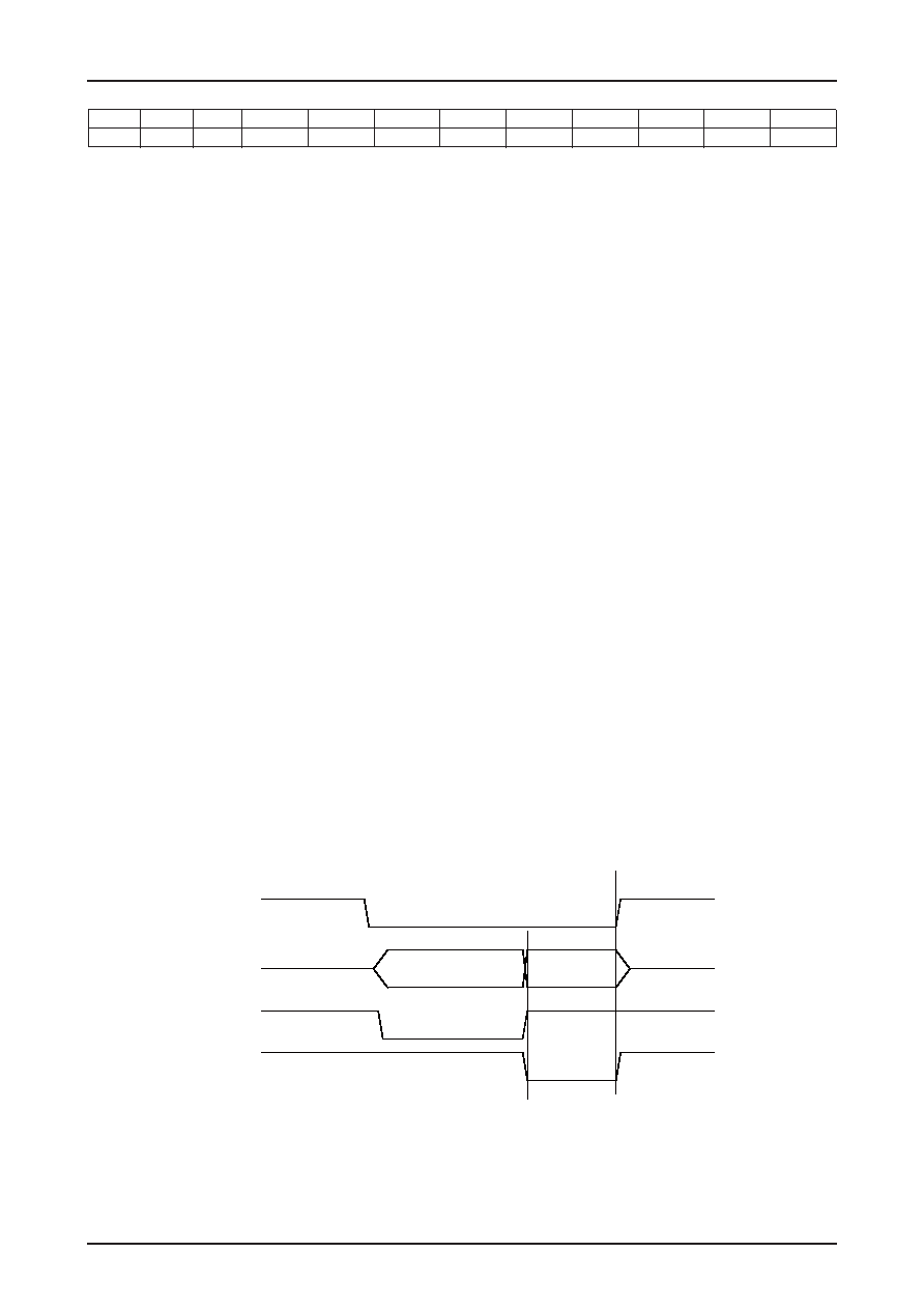
RDY Signal Output Timing
RD
RDY
Timing1
RDY
Timing2
DATn
VALID
OUTPUT
相关PDF资料 |
PDF描述 |
|---|---|
| LA72702NV | SPECIALTY CONSUMER CIRCUIT, PDSO24 |
| LA72702NV | SPECIALTY CONSUMER CIRCUIT, PDSO24 |
| LA72702VA | SPECIALTY CONSUMER CIRCUIT, PDSO24 |
| LA7270 | 2 CHANNEL, VIDEO PREAMPLIFIER, PDIP22 |
| LA7270M | 2 CHANNEL, VIDEO PREAMPLIFIER, PDSO24 |
相关代理商/技术参数 |
参数描述 |
|---|---|
| LA72700V-MPB-E | 制造商:ON Semiconductor 功能描述:VIDEO ICS - Ammo Pack |
| LA72700V-N-MPB-E | 制造商:ON Semiconductor 功能描述:VIDEO ICS - Ammo Pack |
| LA72700V-N-TLM-E | 制造商:ON Semiconductor 功能描述:VIDEO ICS - Tape and Reel 制造商:ON Semiconductor 功能描述:REEL / VIDEO ICS |
| LA72702NV | 制造商:SANYO 制造商全称:Sanyo Semicon Device 功能描述:Monolithic Linear IC For US TV BTSC Decoder |
| LA72702NV-MPB-E | 功能描述:编码器、解码器、复用器和解复用器 RoHS:否 制造商:Micrel 产品:Multiplexers 逻辑系列:CMOS 位数: 线路数量(输入/输出):2 / 12 传播延迟时间:350 ps, 400 ps 电源电压-最大:2.625 V, 3.6 V 电源电压-最小:2.375 V, 3 V 最大工作温度:+ 85 C 安装风格:SMD/SMT 封装 / 箱体:QFN-44 封装:Tray |
发布紧急采购,3分钟左右您将得到回复。