- 您现在的位置:买卖IC网 > PDF目录95590 > LA7956 4-CHANNEL, AUDIO/VIDEO SWITCH, SIP9 PDF资料下载
参数资料
| 型号: | LA7956 |
| 元件分类: | 多路复用及模拟开关 |
| 英文描述: | 4-CHANNEL, AUDIO/VIDEO SWITCH, SIP9 |
| 封装: | SIP-9 |
| 文件页数: | 4/4页 |
| 文件大小: | 94K |
| 代理商: | LA7956 |
LA7956
PS No. 3353-4/4
SANYO Semiconductor Co.,Ltd. assumes no responsibility for equipment failures that result from using
products at values that exceed, even momentarily, rated values (such as maximum ratings, operating condition
ranges, or other parameters) listed in products specifications of any and all SANYO Semiconductor Co.,Ltd.
products described or contained herein.
SANYO Semiconductor Co.,Ltd. strives to supply high-quality high-reliability products, however, any and all
semiconductor products fail or malfunction with some probability. It is possible that these probabilistic failures or
malfunction could give rise to accidents or events that could endanger human lives, trouble that could give rise
to smoke or fire, or accidents that could cause damage to other property. When designing equipment, adopt
safety measures so that these kinds of accidents or events cannot occur. Such measures include but are not
limited to protective circuits and error prevention circuits for safe design, redundant design, and structural
design.
Upon using the technical information or products described herein, neither warranty nor license shall be granted
with regard to intellectual property rights or any other rights of SANYO Semiconductor Co.,Ltd. or any third
party. SANYO Semiconductor Co.,Ltd. shall not be liable for any claim or suits with regard to a third party's
intellctual property rights which has resulted from the use of the technical information and products mentioned
above.
Information (including circuit diagrams and circuit parameters) herein is for example only; it is not guaranteed
for volume production.
Any and all information described or contained herein are subject to change without notice due to
product/technology improvement, etc. When designing equipment, refer to the "Delivery Specification" for the
SANYO Semiconductor Co.,Ltd. product that you intend to use.
In the event that any or all SANYO Semiconductor Co.,Ltd. products described or contained herein are
controlled under any of applicable local export control laws and regulations, such products may require the
export license from the authorities concerned in accordance with the above law.
No part of this publication may be reproduced or transmitted in any form or by any means, electronic or
mechanical, including photocopying and recording, or any information storage or retrieval system, or otherwise,
without the prior written consent of SANYO Semiconductor Co.,Ltd.
Design Notes
An improvement in the DC clamp circuit has improved the sync signal compression attributable to the signal source
impedance, but the response time of the DC clamp is made longer accordingly than that of the LA7952. Make
adjustments by connecting a high resistance (several hundred k
Ω) across input pin and GND (decreasing the resistance
makes the sync signal compression larger).
This catalog provides information as of May, 2008. Specifications and information herein are subject to change
without notice.
10M
35
40
45
50
55
60
65
70
75
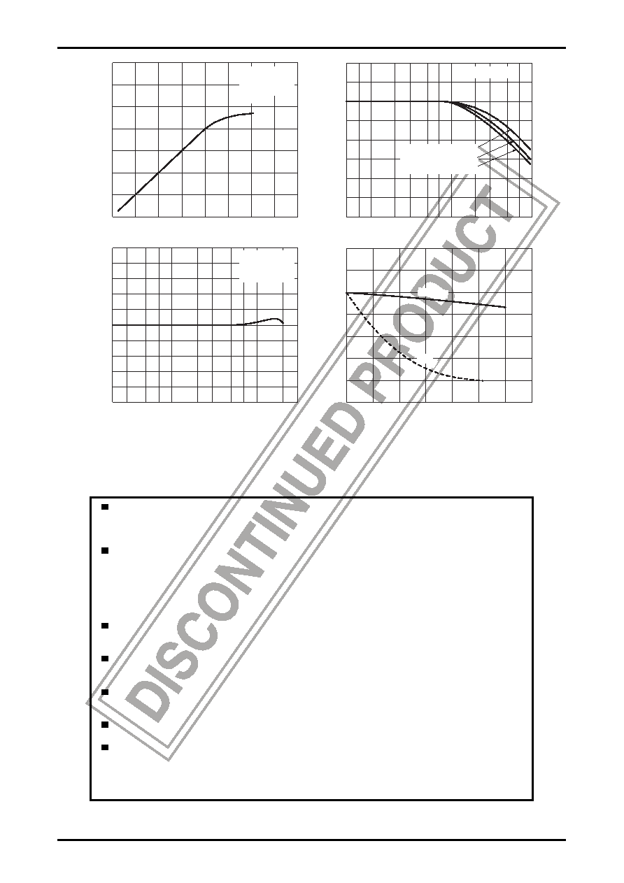
CT -- f
Frequency, f -- Hz
Crosstalk,CT
-
-dB
JK795607
57 100k
23
5
7
1M
23
5
7
Pin 4 input, pin 6 output
Pin 6 input, pin 8 output
Pin 8 input, pin 9 output
VCC = 12V
1400
-100
-80
-60
-40
-20
0
20
40
Sync Signal Compression Ratio
Input Series Resistance, R2N -- Ω
Sync
Signal
Compression
Rati
(Ration
of
compression
to
that
at
R
IN
=
0Ω)
JK795609
5
200
400
600
800
100
1200
LA7956
LA7952
4
0
3.5
3.0
2.5
2.0
1.5
1.0
0.5
Input/ Output Characteristic
Input -- Vp-p
Output
-
Vp-p
JK795606
5123
VCC = 12V
Pin 4 input
Frequency
15kHz
3
-10
-8
-6
-4
-2
0
2
4
6
8
10
Frequency Characteristic
Frequency, f -- Hz
Attenuation
-
-dB
JK795608
2
3
5
7
1M
2
3
5
7 10M
2
VCC = 12V
Pin 4 input
Input 1Vp-p
相关PDF资料 |
PDF描述 |
|---|---|
| LA8128T | SPECIALTY ANALOG CIRCUIT, PDSO8 |
| LA8160V | SPECIALTY ANALOG CIRCUIT, PDSO16 |
| LA8632M | COMPANDER, PDSO24 |
| LA8632 | COMPANDER, PDIP24 |
| LA8633V | COMPANDER, PDSO24 |
相关代理商/技术参数 |
参数描述 |
|---|---|
| LA7957 | 制造商:SANYO 制造商全称:Sanyo Semicon Device 功能描述:Video Switch for TV/VCR Use |
| LA7958 | 制造商:SANYO 制造商全称:Sanyo Semicon Device 功能描述:For TV, VTR Audio/Video Switch |
| LA7958_11 | 制造商:SANYO 制造商全称:Sanyo Semicon Device 功能描述:Audio/Video Switch |
| LA7958N-E | 制造商:ON Semiconductor 功能描述:AV SW IC - Ammo Pack 制造商:ON Semiconductor 功能描述:FNFLD / AV SW IC |
| LA7958N-LG-E | 功能描述:视频开关 IC AV SW IC RoHS:否 制造商:Texas Instruments 开关数量:4 开启电阻(最大值):12 Ohms 传播延迟时间: 开启时间(最大值): 关闭时间(最大值): 最大工作温度:+ 85 C 最小工作温度:- 40 C 封装 / 箱体:WQFN-42 封装:Reel |
发布紧急采购,3分钟左右您将得到回复。