- 您现在的位置:买卖IC网 > PDF目录30728 > LA9250M SPECIALTY CONSUMER CIRCUIT, PQFP64 PDF资料下载
参数资料
| 型号: | LA9250M |
| 元件分类: | 消费家电 |
| 英文描述: | SPECIALTY CONSUMER CIRCUIT, PQFP64 |
| 封装: | QIP-64 |
| 文件页数: | 11/17页 |
| 文件大小: | 152K |
| 代理商: | LA9250M |
No. 5981-3/17
LA9250M
Continued from preceding page.
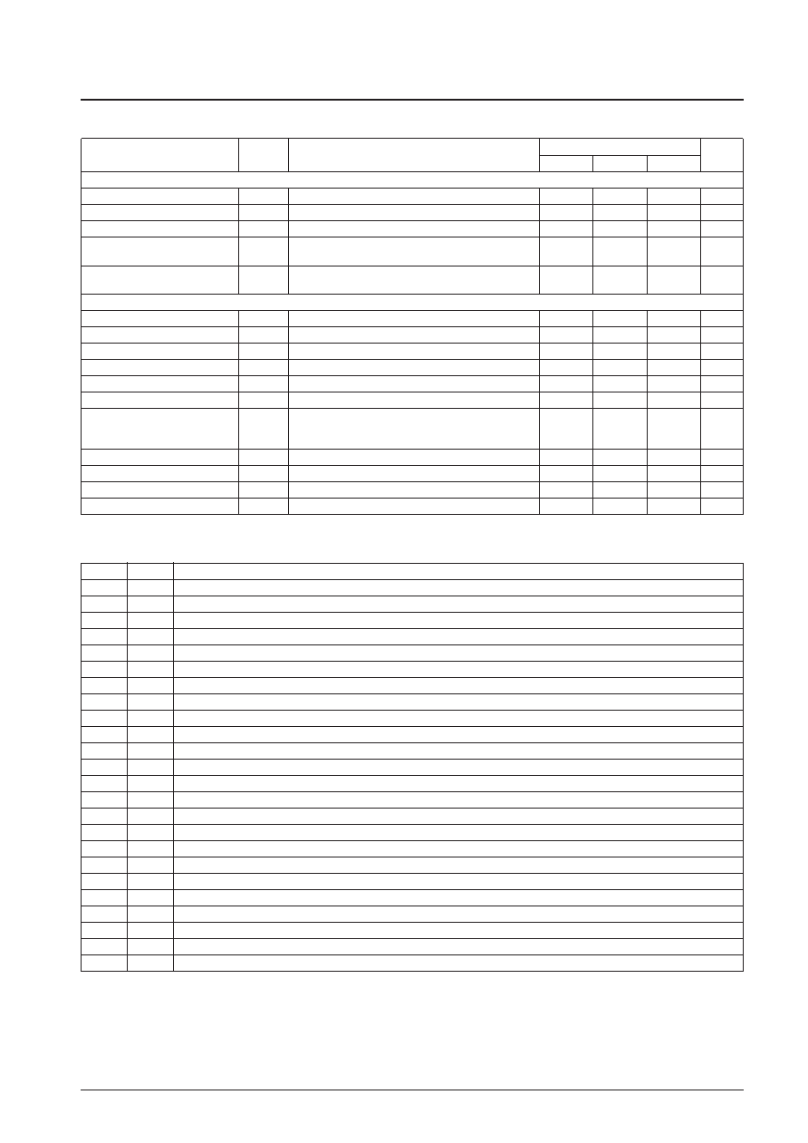
Parameter
Symbol
Conditions
Ratings
Unit
min
typ
max
[Spindle Amplifier]
Offset 12
SPD12ost At SPD, the difference from VR, SP8 = 0 V: 12 cm mode
–40
0
+40
mV
Offset 8
SPD8ost
At SPD, the difference from VR, SP8 = 3 V: 8 cm mode
–40
0
+40
mV
Offset off
SPDof
At SPD, the difference from VR, SP8 = 3 V: 8 cm mode
–40
0
+40
mV
Output voltage H12
SPD-H12
The difference from offset 12,
0.35
0.50
0.65
V
SP8 = 0 V, 12 cm mode, CLV = 3 V
Output voltage H8
SPD-H8
The difference from offset 8,
0.10
0.20
0.30
V
SP8 = 3 V, 8 cm mode, CLV = 3 V
[Sled Amplifier]
Offset SLD
SLDost
SLEQ = VR, the difference from VR
–80
0
+80
mV
Offset off
SLDof
SLOF = High
–40
0
+40
mV
SLC no-signal voltage
SLCo
SLC
1.0
1.5
2.0
V
Shock no-signal voltage
SCIo
SCI, the difference from VR
–40
0
+40
mV
Shock detection voltage (high)
SCIvthH
SCI, the difference from VR
90
140
190
mV
Shock detection voltage (low)
SCIvthL
SCI, the difference from VR
–190
–140
–90
mV
The difference between the LF2 voltage when DEF is
DEF detection voltage
DEFvth
detected with RF = 1.9 V and the LF2 voltage when
0.20
0.35
0.50
V
RF = 1.9 V.
DEF output voltage (high)
DEF-H
2.5
2.9
V
DEF output voltage (low)
DEF-L
0
0.5
V
APC reference voltage
LDS
The LDS voltage such that LDD = 1.5 V
120
170
220
mV
APC off voltage
LDDof
LDD
2.7
2.9
V
Pin Functions
Pin No.
Pin
Function
1
FIN2
Pickup photodiode (focus, RF) connection
2
FIN1
Pickup photodiode (focus, RF) connection
3
E
Pickup photodiode (tracking) connection
4
F
Pickup photodiode (tracking) connection
5
TB
TE signal DC component input. Pickup photodiode (tracking) connection
6TE–
TE signal gain setting resistor connection. A resistor is connected between this pin and TE.
7
TE
TE signal output
8
TESI
TES comparator input. Takes the bandpass filtered TE signal as its input.
9
SCI
Shock detection input
10
TH
Tracking gain time constant setting
11
TA
TA amplifier output
12
TD–
In conjunction with the TD and VR pins, used to form the tracking phase compensation circuit constant
13
TD
Tracking phase compensation setting
14
JP
Track jump signal amplitude setting
15
TO
Tracking control signal output
16
(NC)
No connection
17
FD
Focusing control signal output
18
FD–
In conjunction with the FD and FA pins, used to form the focusing phase compensation circuit constant
19
FA
In conjunction with the FD- and FA- pins, used to form the focusing phase compensation circuit constant
20
FA–
In conjunction with the FA and FE pins, used to form the focusing phase compensation circuit constant
21
FE
FE signal output
22
FE–
FE signal gain setting resistor connection. A resistor is connected between this pin and FE.
23
SP
CLV pin input signal inverted output
24
SPG
Gain setting resistor connection (12 cm spindle mode)
Continued on next page.
相关PDF资料 |
PDF描述 |
|---|---|
| LA9251M | SPECIALTY CONSUMER CIRCUIT, PQFP64 |
| LA9410 | 2 CHANNEL, AUDIO AMPLIFIER, PDIP28 |
| LA9511W | SPECIALTY CONSUMER CIRCUIT, PQFP48 |
| LA9520V | SPECIALTY CONSUMER CIRCUIT, PDSO36 |
| LA9613T | SPECIALTY CONSUMER CIRCUIT, PDSO36 |
相关代理商/技术参数 |
参数描述 |
|---|---|
| LA9251 | 制造商:SANYO 制造商全称:Sanyo Semicon Device 功能描述:CD Player Analog Signal Processor (ASP) |
| LA9251M | 制造商:SANYO 制造商全称:Sanyo Semicon Device 功能描述:CD Player Analog Signal Processor (ASP) |
| LA92B-2EG-1 | 制造商:LIGITEK 制造商全称:LIGITEK electronics co., ltd. 功能描述:LED ARRAY |
| LA92B-2EG-2 | 制造商:LIGITEK 制造商全称:LIGITEK electronics co., ltd. 功能描述:LED ARRAY |
| LA92B-2EG-2-AS-PF | 制造商:LIGITEK 制造商全称:LIGITEK electronics co., ltd. 功能描述:LED ARRAY |
发布紧急采购,3分钟左右您将得到回复。