- 您现在的位置:买卖IC网 > PDF目录65794 > LB11988N AC MOTOR CONTROLLER, 1.3 A, PDIP18 PDF资料下载
参数资料
| 型号: | LB11988N |
| 元件分类: | 运动控制电子 |
| 英文描述: | AC MOTOR CONTROLLER, 1.3 A, PDIP18 |
| 封装: | 0.300 INCH, DIP-18 |
| 文件页数: | 3/6页 |
| 文件大小: | 135K |
| 代理商: | LB11988N |
No. 7118-3/6
LB11988N
Truth Table and Control Function
Note: The “H” state for FR is defined as a voltage of 8 V or higher, and the “L”
state for FR is defined as a voltage of 4 V or lower (when VCC is 12 V).
Note: For the Hall inputs, the input “H” state means the state in which the (+)
input for that phase is at least 0.01 V higher than the (–) input for that
phase. Similarly, the “L” state means the state in which the (+) input for
that phase is at least 0.01 V lower than the (–) input for the that phase.
Note: Since this drive system adopts a 180° current application technique,
phases other than the sink and source phase will not necessarily go to
the off state.
Source → sink
Hall input
FR
UV
W
1
V → W
HH
L
H
W → VL
2
U → W
HL
L
H
W → UL
3
U → V
HLH
H
V → UL
4
W → V
LL
H
V → WL
5
W → U
LH
H
U → WL
6
V → U
LHL
H
U → VL
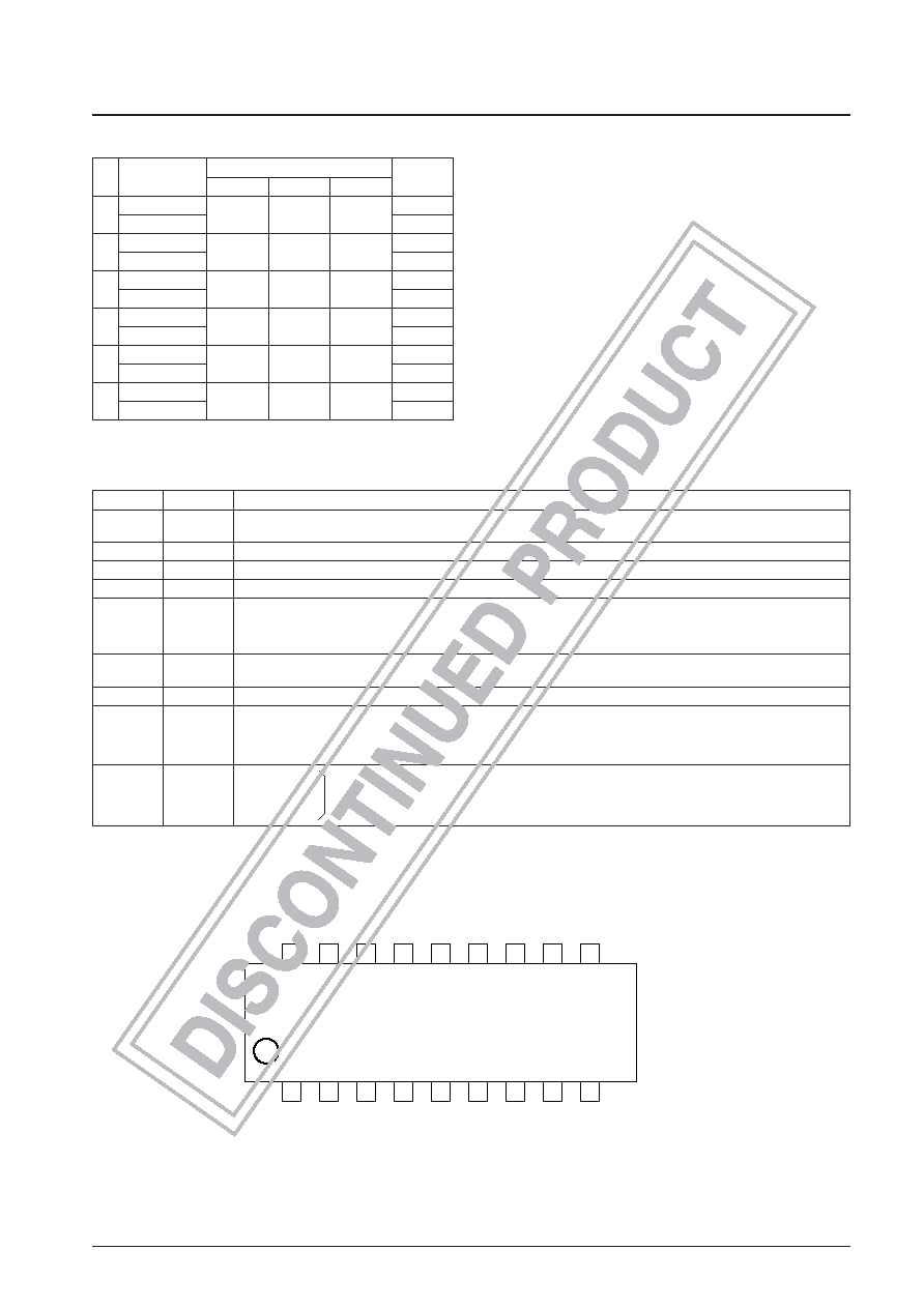
Pin Functions
Pin Assignments
Pin
Pin No.
Pin function
GND
5
Ground for circuits other than the output transistors.
The lowest potential of the output transistors will be that of the RF pin.
FG-OUT
3
FG comparator output
FR
4
Forward/reverse direction switching input
FC
6
Corrects the frequency characteristics of the saturation prevention circuit and the current limiter circuit.
UIN+, UIN–
7, 8
U phase Hall element input. The logic high level indicates the state IN+ > IN–.
VIN+, VIN–
9, 10
V phase Hall element input. The logic high level indicates the state IN+ > IN–.
WIN+, WIN–
11, 12
W phase Hall element input. The logic high level indicates the state IN+ > IN–.
VCC
13
Power supply for IC internal circuits other than the output block.
This voltage must be stabilized so that ripple and noise do not enter the IC.
VS
14
Output block power supply
Output current detection. The current limiter circuit operates using the resistor Rf connected between this pin and ground.
Rf
15
The lower side saturation prevention circuit operates according to the voltage that appears on this pin. Since the saturation
prevention level is set with this voltage, the operation of the low side saturation prevention circuit will become less sensitive if
the value of the resistor Rf is reduced excessively.
UOUT
17
U phase output
VOUT
18
V phase output
(Spark killer diodes are built in the output circuits.)
WOUT
1
W phase output
14
12
10
11
13
9
1
2
3
4
5
6
7
8
NC
W
OUT
15
16
17
18
FG
OUT
FR
GND
FC
U
IN
+
U
IN
—
V
IN
+
V
IN
—
W
IN
+
W
IN
—
V
CC
VS
RF
NC
U
OUT
V
OUT
Top view
LB11988N
相关PDF资料 |
PDF描述 |
|---|---|
| LB11997H | DISK DRIVE MOTOR CONTROLLER, 1.3 A, PDSO28 |
| LB1256M | SPECIALTY ANALOG CIRCUIT, PDSO20 |
| LB1634M | BRUSH DC MOTOR CONTROLLER, PDSO16 |
| LB1657M | STEPPER MOTOR CONTROLLER, 0.5 A, PDSO16 |
| LB1674M | BRUSHLESS DC MOTOR CONTROLLER, 0.6 A, PDSO24 |
相关代理商/技术参数 |
参数描述 |
|---|---|
| LB11988V | 制造商:SANYO 制造商全称:Sanyo Semicon Device 功能描述:Fan Motor Driver |
| LB11988V_12 | 制造商:SANYO 制造商全称:Sanyo Semicon Device 功能描述:Monolithic Digital IC Fan Motor Driver |
| LB11988V-MPB-E | 功能描述:马达/运动/点火控制器和驱动器 RoHS:否 制造商:STMicroelectronics 产品:Stepper Motor Controllers / Drivers 类型:2 Phase Stepper Motor Driver 工作电源电压:8 V to 45 V 电源电流:0.5 mA 工作温度:- 25 C to + 125 C 安装风格:SMD/SMT 封装 / 箱体:HTSSOP-28 封装:Tube |
| LB11988V-TLM-E | 功能描述:马达/运动/点火控制器和驱动器 BRUSHLESS MOTOR DRIVER RoHS:否 制造商:STMicroelectronics 产品:Stepper Motor Controllers / Drivers 类型:2 Phase Stepper Motor Driver 工作电源电压:8 V to 45 V 电源电流:0.5 mA 工作温度:- 25 C to + 125 C 安装风格:SMD/SMT 封装 / 箱体:HTSSOP-28 封装:Tube |
| LB11990W | 制造商:SANYO 制造商全称:Sanyo Semicon Device 功能描述:Three-Phase Brushless Motor Driver |
发布紧急采购,3分钟左右您将得到回复。