- 您现在的位置:买卖IC网 > PDF目录80209 > LB1662M BRUSHLESS DC MOTOR CONTROLLER, 1.5 A, PDSO16 PDF资料下载
参数资料
| 型号: | LB1662M |
| 元件分类: | 运动控制电子 |
| 英文描述: | BRUSHLESS DC MOTOR CONTROLLER, 1.5 A, PDSO16 |
| 封装: | 0.300 INCH, MFP-16 |
| 文件页数: | 5/6页 |
| 文件大小: | 97K |
| 代理商: | LB1662M |
LB1662D, 1662M
No.3416-5/6
Usage Notes (See the Sample Application Circuits.)
(1) Supply voltage (VIN pin)
Use these ICs with the voltage applied between VIN and ground in the range from 3.8 to 6.0V. The current
consumption, ICC, at the VIN pin is from 1.4 to 3.7mA (when VIN = 4.3V). Insert diode D1 to keep coil kickback out
of the power line.
This diode also prevents breakdown due to reverse connections. Also, inserting R1 limits the reverse connection
current flowing into ground and VIN. These ICs have a reverse connection withstand current, ICC = 200mA. Check
R1 around the range from 50 to 200
Ω.
(2) Hall input pin voltage (IN- and IN+ pins)
Set the voltage levels of the input pin for the Hall element output and the Hall element output voltage to within the
range of 0V to VIN-1.5 V.
The gain between the Hall input pin and the output pin is 100dB or greater. The offset voltage of the Hall input amp is
±7mV. Therefore, the Hall element output must be set with the offset voltage (±7mV) considered.
(3) Output transistors (OUT1 and OUT2 pins)
Output Current IO = 1.5A max
Output saturation voltage VOsat = 1.15V/1.0A (typ)
The LB1662D, 1662M requires one of the three types of output protection.
1) When external capacitors are connected between OUT and ground, the capacitance should not exceed 10
μF. Use
capacitance that will hold kickback voltage and back voltage to 80V or less.
2) When external Zener diodes are connected, use one that will have a cutoff voltage of 65V or less. If radio noise is a
problem, insert a 0.01
μF to 0.1μF capacitor between B1 and B2.
3) When external capacitors are connected between OUT and B, use one that will hold kickback voltage to 65V or less.
If it oscillates, insert resistance in series with the capacitor.
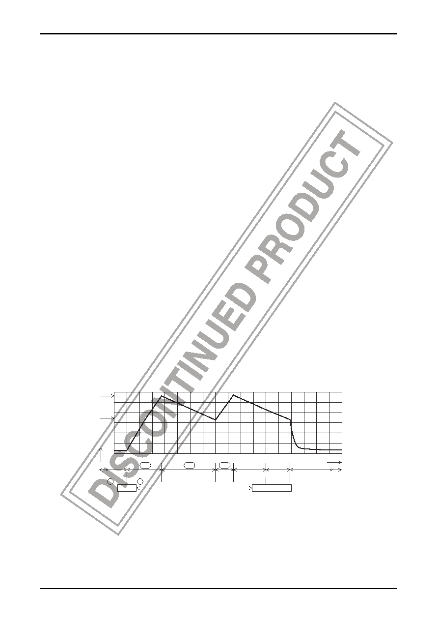
(4) Output protection function (C pin)
Capacitor pin used in forming an automatic return circuit.
If rotation is stopped due to overload, the pin voltage increases and then forces the output to become inactive. In this
case, after proper load adjustment, the output returns to the “drive” mode from the “stop” mode automatically. By
changing the capacitor value, the lock detect time period can be set.
Automatic return circuit C pin voltage
For 1
μF
lock detection time about 1 seconds
lock protection time (output ON) about 0.5 second
(output OFF) about 3.5 seconds
VTH2
VTH1
01
t3
23456789
10
11
12
13
14
15
16
17
t2
t1
1
t (s)
V
C
(V)
Output on
Lock
Output off
Output
on
Rotation
Lock released
2
Output off
相关PDF资料 |
PDF描述 |
|---|---|
| LM1001-7EPD3 | 1-OUTPUT 50 W AC-DC REG PWR SUPPLY MODULE |
| LM1001-7ERD0AH | 1-OUTPUT 50 W AC-DC REG PWR SUPPLY MODULE |
| LM1001-7ERV3 | 1-OUTPUT 50 W AC-DC REG PWR SUPPLY MODULE |
| LM1001-7PD7AHF | 1-OUTPUT 50 W AC-DC REG PWR SUPPLY MODULE |
| LM1001-7PV0AF | 1-OUTPUT 50 W AC-DC REG PWR SUPPLY MODULE |
相关代理商/技术参数 |
参数描述 |
|---|---|
| LB1663 | 制造商:SANYO 制造商全称:Sanyo Semicon Device 功能描述:2-Phase Unipolar Brushless Motor Drivers |
| LB1663-E | 功能描述:马达/运动/点火控制器和驱动器 RoHS:否 制造商:STMicroelectronics 产品:Stepper Motor Controllers / Drivers 类型:2 Phase Stepper Motor Driver 工作电源电压:8 V to 45 V 电源电流:0.5 mA 工作温度:- 25 C to + 125 C 安装风格:SMD/SMT 封装 / 箱体:HTSSOP-28 封装:Tube |
| LB1663M | 制造商:SANYO 制造商全称:Sanyo Semicon Device 功能描述:2-Phase Unipolar Brushless Motor Drivers |
| LB1664N | 制造商:SANYO 制造商全称:Sanyo Semicon Device 功能描述:2-Phase Unipolar Brushless Motor Drivers |
| LB1664N-E | 制造商:Sony Semiconductor Solutions Division 功能描述: |
发布紧急采购,3分钟左右您将得到回复。