- 您现在的位置:买卖IC网 > PDF目录67755 > LB1923M BRUSHLESS DC MOTOR CONTROLLER, 0.03 A, PQFP44 PDF资料下载
参数资料
| 型号: | LB1923M |
| 元件分类: | 运动控制电子 |
| 英文描述: | BRUSHLESS DC MOTOR CONTROLLER, 0.03 A, PQFP44 |
| 封装: | QFP-44 |
| 文件页数: | 17/19页 |
| 文件大小: | 152K |
| 代理商: | LB1923M |
LB1923M
No.6067-7/19
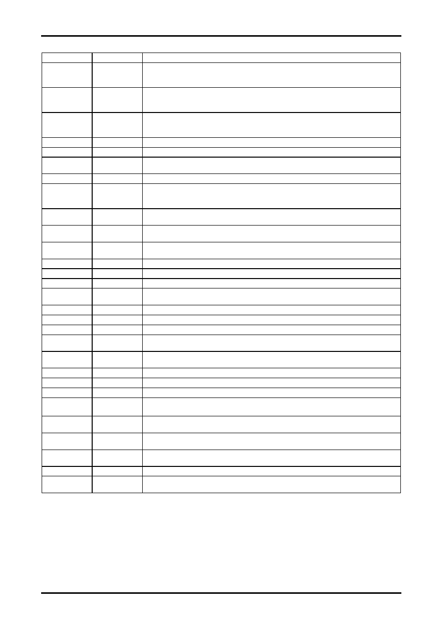
Pin Functions
Pin
Pin No
Function
IN1+, IN1-
IN2+, IN2-
IN3+, IN3-
19, 20
21, 22
23, 24
Hall inputs for the phases
The logic high level corresponds to the state VIN+ > VIN-.
UH
VH
WH
27
29
31
Outputs. These are fixed-current source outputs.
UL
VL
WL
26
28
30
The duty is controlled by the output pin PWM.
These are open collector sink outputs.
VCC
32
A capacitor must be inserted between this pin and ground to prevent noise entering the circuit.
VREG
33
7-V shunt regulator output
GND
16 to 18
38 to 40
Ground
CR
34
Used to set the PWM circuit oscillator frequency.
CROCK
35
Motor lock protection circuit. Reference signal oscillator connection. Used by the circuit that prevents
incorrect operation if the clock line is disconnected.
A capacitor must be inserted between this pin and ground.
R
36
VCO circuit. This pin sets the charge and discharge current. A resistor must be inserted between this pin
and ground.
C
37
VCO oscillator connection. A capacitor must be inserted between this pin and ground. Select a value for that
capacitor such that the C pin oscillator frequency does not exceed 1MHz.
FILI
42
Inverting input to the VCO filter amplifier. This pin is connected to the VCO PLL through an (IC internal)
10k
resistor.
FILO
41
VCO filter amplifier output. This pin is connected to the VCO circuit internally.
DOUT
3
Speed discriminator output. A low level is output when the motor is over speed.
ROUT
4
PLL circuit output. Outputs the result of the phase comparison between 1/2fCLK and 1/2fFG.
LD
5
Lock detection output. This is an open collector output.
This pin outputs a low level when the motor speed is within the locked range (±6.25%).
INTREF
43
Integrating amplifier noninverting input (the 1/2 VCC potential)
INTIN
2
Integrating amplifier inverting input
INTOUT
1
Integrating amplifier output
TOC
44
Torque command input. Normally, this pin is connected to the INTOUT pin. Lowering the TOC pin potential
increases the torque by changing the PWM signal duty for the UL, VL, and WL outputs.
FGIN+
15
FG amplifier noninverting input (the 1/2 VCC potential). A capacitor must be inserted between this pin and
ground.
FGIN-
14
FG amplifier inverting input
FGOUT
13
FG amplifier output
FGSOUT
12
FG amplifier (post-Schmitt) output. This is an open collector output.
RF
25
Output current detection. A resistor must be inserted between this pin and ground.
This resistor sets the maximum output current IOUT to be 0.5/Rf.
S/S
9
Start/stop control input. Apply a low level for start, and either a high level or an open (high-impedance) state
for start.
F/R
7
Forward/reverse control input. Apply a low level for forward, and either a high level or an open (high-
impedance) state for reverse.
BR
6
Braking control input (short braking operation). Apply a low level for start, and either a high level or an open
(highimpedance) state to brake the motor.
CLK
8
External clock signal input. 10kHz max.
N1
N2
10
11
Speed discriminator count value selection inputs
相关PDF资料 |
PDF描述 |
|---|---|
| LB1946 | STEPPER MOTOR CONTROLLER, 1.75 A, PDFM28 |
| LC5511D | POWER FACTOR CONTROLLER, 18 kHz SWITCHING FREQ-MAX, DIP7 |
| LC5521D | 2.5 A POWER FACTOR CONTROLLER, 18 kHz SWITCHING FREQ-MAX, DIP7 |
| LC72137 | PLL FREQUENCY SYNTHESIZER, 40 MHz, PDIP22 |
| LC72137M | PLL FREQUENCY SYNTHESIZER, 40 MHz, PDSO20 |
相关代理商/技术参数 |
参数描述 |
|---|---|
| LB1923M-MPB-E | 制造商:ON Semiconductor 功能描述:3PHASE MOTOR PRE-DRIVER - Trays |
| LB1923M-TLM-E | 功能描述:马达/运动/点火控制器和驱动器 RoHS:否 制造商:STMicroelectronics 产品:Stepper Motor Controllers / Drivers 类型:2 Phase Stepper Motor Driver 工作电源电压:8 V to 45 V 电源电流:0.5 mA 工作温度:- 25 C to + 125 C 安装风格:SMD/SMT 封装 / 箱体:HTSSOP-28 封装:Tube |
| LB1924 | 制造商:SANYO 制造商全称:Sanyo Semicon Device 功能描述:Power Brushless Motor Driver IC for Office Automation Equipment |
| LB1927 | 制造商:SANYO 制造商全称:Sanyo Semicon Device 功能描述:For Office Automation Equipment 3-phase Brushless Motor Driver |
| LB1927-E | 功能描述:马达/运动/点火控制器和驱动器 RoHS:否 制造商:STMicroelectronics 产品:Stepper Motor Controllers / Drivers 类型:2 Phase Stepper Motor Driver 工作电源电压:8 V to 45 V 电源电流:0.5 mA 工作温度:- 25 C to + 125 C 安装风格:SMD/SMT 封装 / 箱体:HTSSOP-28 封装:Tube |
发布紧急采购,3分钟左右您将得到回复。