- 您现在的位置:买卖IC网 > PDF目录30729 > LB8901M SPECIALTY CONSUMER CIRCUIT, PDSO24 PDF资料下载
参数资料
| 型号: | LB8901M |
| 元件分类: | 消费家电 |
| 英文描述: | SPECIALTY CONSUMER CIRCUIT, PDSO24 |
| 封装: | MFP-24 |
| 文件页数: | 3/5页 |
| 文件大小: | 65K |
| 代理商: | LB8901M |
LB8901M
No.3030–3/5
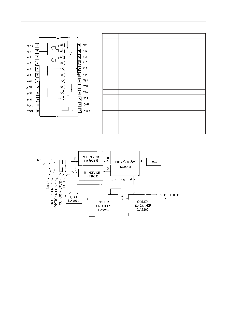
Pin Function
.
o
N
n
i
Pe
m
a
N
n
i
Pn
o
i
t
p
i
r
c
s
e
D
n
i
P
1
2
V C
C 2
V C
C 1
3
,
1
t
a
e
s
l
u
p
t
f
i
h
s
e
m
a
r
f
r
o
f
y
l
p
u
s
r
e
w
o
P
3
,
1
t
a
e
s
l
u
p
e
u
l
a
v
-
e
r
h
t
r
o
f
y
l
p
u
s
r
e
w
o
P
3
4
5
6
1
2
3
4
D
C
f
o
1
r
o
f
,
t
u
p
t
u
o
e
v
i
r
d
e
u
l
a
v
-
e
r
h
t
e
v
i
t
i
s
o
P
D
C
f
o
3
r
o
f
,
t
u
p
t
u
o
e
v
i
r
d
e
u
l
a
v
-
e
r
h
t
e
v
i
t
i
s
o
P
D
C
f
o
2
r
o
f
,
t
u
p
t
u
o
e
v
i
r
d
e
u
l
a
v
-
o
w
t
e
v
i
t
i
s
o
P
D
C
f
o
4
r
o
f
,
t
u
p
t
u
o
e
v
i
r
d
e
u
l
a
v
-
o
w
t
e
v
i
t
i
s
o
P
7
8
9
0
1
4
S
1
S
2
S
3
S
D
C
f
o
4
S
r
o
f
,
t
u
p
t
u
o
e
v
i
r
d
e
u
l
a
v
-
o
w
t
e
v
i
t
i
s
o
P
D
C
f
o
1
S
r
o
f
,
t
u
p
t
u
o
e
v
i
r
d
e
u
l
a
v
-
o
w
t
e
v
i
t
i
s
o
P
D
C
f
o
2
S
r
o
f
,
t
u
p
t
u
o
e
v
i
r
d
e
u
l
a
v
-
o
w
t
e
v
i
t
i
s
o
P
D
C
f
o
3
S
r
o
f
,
t
u
p
t
u
o
e
v
i
r
d
e
u
l
a
v
-
o
w
t
e
v
i
t
i
s
o
P
1
2
1
3
1
V C
C 3
V C
C 4
V C
C 5
4
,
2
r
o
f
y
l
p
u
s
r
e
w
o
P
4
S
,
3
S
r
o
f
y
l
p
u
s
r
e
w
o
P
2
S
,
1
S
r
o
f
y
l
p
u
s
r
e
w
o
P
4
1D
N
Gn
i
p
d
n
u
o
r
G
5
1
6
1
7
1
8
1
VS3
VS2
VS1
VS4
r
e
v
i
r
d
3
S
r
o
f
t
u
p
n
i
k
c
o
l
C
r
e
v
i
r
d
2
S
r
o
f
t
u
p
n
i
k
c
o
l
C
r
e
v
i
r
d
1
S
r
o
f
t
u
p
n
i
k
c
o
l
C
r
e
v
i
r
d
4
S
r
o
f
t
u
p
n
i
k
c
o
l
C
9
1
0
2
1
2
VI4
VI2
VI3
VI1
r
e
v
i
r
d
4
r
o
f
t
u
p
n
i
k
c
o
l
C
r
e
v
i
r
d
2
r
o
f
t
u
p
n
i
k
c
o
l
C
r
e
v
i
r
d
3
r
o
f
t
u
p
n
i
k
c
o
l
C
r
e
v
i
r
d
1
r
o
f
t
u
p
n
i
k
c
o
l
C
3
2
4
2
V S
I
V F
I
r
e
v
i
r
d
3
r
o
f
t
u
p
n
i
e
s
l
u
p
e
u
l
a
v
-
e
r
h
T
r
e
v
i
r
d
1
r
o
f
t
u
p
n
i
e
s
l
u
p
e
u
l
a
v
-
e
r
h
T
Sample Application Circuit : Camera Block Diagram
Proper Cares to be Taken in Designing a Printed Circuit Board
The LB8901M draws a large instantaneous current when it drives a load. The LB8901M is also designed to drive a load at
a very high speed. When designing a printed circuit board, keep in mind the following points to prevent the output wave-
forms from being adversely affected.
1) Make the pattern of the power supply, GND lines as large as possible.
2) Place the bypass capacitor as close to the IC as possible (less than 1cm).
3) Make the wiring of the input signal line as short as possible to minimize the effect of stray capacitance.
4) Make the wiring of the output signal line also as short as possible, because the inductance of a long signal line may affect
the output waveforms adversely.
Take such necessary measures that a small resistance is inserted in series with a load.
5) When using a power save circuit, place it also as close to the IC as possible.
Equivalent Circuit Block Diagram
相关PDF资料 |
PDF描述 |
|---|---|
| LB8902M | SPECIALTY CONSUMER CIRCUIT, PDSO16 |
| LB8904M | SPECIALTY CONSUMER CIRCUIT, PDSO30 |
| LC010CL | DC-DC REG PWR SUPPLY MODULE |
| LC015D | DC-DC REG PWR SUPPLY MODULE |
| LC010BK | DC-DC REG PWR SUPPLY MODULE |
相关代理商/技术参数 |
参数描述 |
|---|---|
| LB8902 | 制造商:SANYO 制造商全称:Sanyo Semicon Device 功能描述:3-Channel Clock Driver |
| LB8902M | 制造商:SANYO 制造商全称:Sanyo Semicon Device 功能描述:3-Channel Clock Driver |
| LB8904 | 制造商:SANYO 制造商全称:Sanyo Semicon Device 功能描述:CCD Clock Driver |
| LB8904M | 制造商:SANYO 制造商全称:Sanyo Semicon Device 功能描述:CCD Clock Driver |
| LB-891 | 制造商:Ideal Industries Inc 功能描述:TOOLS |
发布紧急采购,3分钟左右您将得到回复。