- 您现在的位置:买卖IC网 > PDF目录30729 > LC0710LG SPECIALTY CONSUMER CIRCUIT, PBGA40 PDF资料下载
参数资料
| 型号: | LC0710LG |
| 元件分类: | 消费家电 |
| 英文描述: | SPECIALTY CONSUMER CIRCUIT, PBGA40 |
| 封装: | 4.40 X 3.60 MM, FLGA-40 |
| 文件页数: | 2/22页 |
| 文件大小: | 426K |
| 代理商: | LC0710LG |

LC72713W
No.6870-10/29
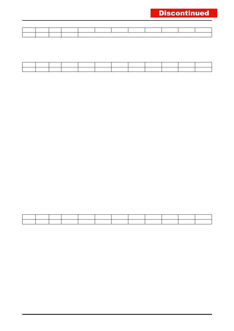
Layer 4 CRC Register
Address
Register
R/W
Initial value
BIT7
BIT6
BIT5
BIT4
BIT3
BIT2
BIT1
BIT0
06H
CRC4
W
00H
(LSB)
This is the data group write register used for the layer 4 CRC check. It is used only when the parallel interface is used.
Applications should specify the dedicated CCB address when using the serial interface.
Status Register
Address
Register
R/W
Initial value
BIT7
BIT6
BIT5
BIT4
BIT3
BIT2
BIT1
BIT0
01H
STAT
R
-
VH
BLK
FRM
ERR
PRI
HEAD
CRC4
*
*: BIT0 is unused.
VH
0: Indicates data for which only horizontal correction was performed.
1: Indicates data for which after horizontal correction, vertical and then second horizontal correction were performed
as well.
BLK
0: Indicates data that was received with block synchronization unsynchronized.
1: Indicates data that was received with block synchronization synchronized.
FRM
0: Indicates data that was received with frame synchronization unsynchronized.
1: Indicates data that was received with frame synchronization synchronized.
ERR
0: Indicates data for which error correction completed and no errors were detected in the level 2 CRC check.
1: Indicates data for which error correction was not possible or for which errors were detected in the level 2 CRC
check.
PRI
0: Indicates data that was inferred to be data block data by the frame synchronization circuit.
1: Indicates data that was inferred to be parity block data by the frame synchronization circuit.
HEAD
0:
1: Indicates data that was inferred to be in the frame head block by the frame synchronization circuit.
This flag is valid only when VH is 0.
CRC4
0: Indicates that the layer 4 CRC detection circuit division registers were not all zeros.
1: Indicates that the layer 4 CRC detection circuit division registers were all zeros, i.e. that there were no errors.
The result at the point immediately prior to register readout is loaded into this flag.
Block Number Register
Address
Register
R/W
Initial value
BIT7
BIT6
BIT5
BIT4
BIT3
BIT2
BIT1
BIT0
02H
BLNO
R
-
BLN7
BLN6
BLN5
BLN4
BLN3
BLN2
BLN1
BLN0
Indicates the block number or the parity block number of the output data.
A single frame consists of data blocks numbered 0 to 189 and parity blocks numbered 0 to 81. Output following
vertical correction does not include parity block data.
The value of the block number register is undefined if VEC_HALT (bit 2 in control register 1) is set to 1.
相关PDF资料 |
PDF描述 |
|---|---|
| LC07410LG | SPECIALTY CONSUMER CIRCUIT, PBGA40 |
| LC07410LG | SPECIALTY CONSUMER CIRCUIT, PBGA40 |
| LC074146LP | 1 CHANNEL, AUDIO/VIDEO AMPLIFIER, QCC40 |
| LC074146LP | 1 CHANNEL, AUDIO/VIDEO AMPLIFIER, QCC40 |
| LC19001A010 | SPECIALTY CONSUMER CIRCUIT, PQFP80 |
相关代理商/技术参数 |
参数描述 |
|---|---|
| LC07410LG | 制造商:SANYO 制造商全称:Sanyo Semicon Device 功能描述:Monaural CODEC + Audio I/F + Video Driver |
| LC074146LP | 制造商:SANYO 制造商全称:Sanyo Semicon Device 功能描述:CMOS IC Monaural CODEC+Audio I/F +Video driver IC |
| LC07422T | 制造商:SANYO 制造商全称:Sanyo Semicon Device 功能描述:CMOS IC Audio CODEC with Video Driver |
| LC07424LP | 制造商:SANYO 制造商全称:Sanyo Semicon Device 功能描述:CMOS IC Audio CODEC with Video Driver |
| LC07424LP-MPB-E | 功能描述:接口—CODEC RoHS:否 制造商:Texas Instruments 类型: 分辨率: 转换速率:48 kSPs 接口类型:I2C ADC 数量:2 DAC 数量:4 工作电源电压:1.8 V, 2.1 V, 2.3 V to 5.5 V 最大工作温度:+ 85 C 安装风格:SMD/SMT 封装 / 箱体:DSBGA-81 封装:Reel |
发布紧急采购,3分钟左右您将得到回复。