- 您现在的位置:买卖IC网 > PDF目录22120 > LC4032B-5T44I (Lattice Semiconductor Corporation)IC PLD 32MC 30I/O 5NS 44TQFP PDF资料下载
参数资料
| 型号: | LC4032B-5T44I |
| 厂商: | Lattice Semiconductor Corporation |
| 文件页数: | 8/99页 |
| 文件大小: | 0K |
| 描述: | IC PLD 32MC 30I/O 5NS 44TQFP |
| 标准包装: | 160 |
| 系列: | ispMACH® 4000B |
| 可编程类型: | 系统内可编程 |
| 最大延迟时间 tpd(1): | 5.0ns |
| 电压电源 - 内部: | 2.3 V ~ 2.7 V |
| 逻辑元件/逻辑块数目: | 2 |
| 宏单元数: | 32 |
| 输入/输出数: | 30 |
| 工作温度: | -40°C ~ 105°C |
| 安装类型: | 表面贴装 |
| 封装/外壳: | 44-TQFP |
| 供应商设备封装: | 44-TQFP(10x10) |
| 包装: | 托盘 |
第1页第2页第3页第4页第5页第6页第7页当前第8页第9页第10页第11页第12页第13页第14页第15页第16页第17页第18页第19页第20页第21页第22页第23页第24页第25页第26页第27页第28页第29页第30页第31页第32页第33页第34页第35页第36页第37页第38页第39页第40页第41页第42页第43页第44页第45页第46页第47页第48页第49页第50页第51页第52页第53页第54页第55页第56页第57页第58页第59页第60页第61页第62页第63页第64页第65页第66页第67页第68页第69页第70页第71页第72页第73页第74页第75页第76页第77页第78页第79页第80页第81页第82页第83页第84页第85页第86页第87页第88页第89页第90页第91页第92页第93页第94页第95页第96页第97页第98页第99页
�� �
�
�Lattice� Semiconductor�
�ispMACH� 4000V/B/C/Z� Family� Data� Sheet�
�?�
�?�
�?�
�?�
�?�
�?�
�Block� CLK2�
�Block� CLK3�
�PT� Clock�
�PT� Clock� Inverted�
�Shared� PT� Clock�
�Ground�
�Clock� Enable� Multiplexer�
�Each� macrocell� has� a� 4:1� clock� enable� multiplexer.� This� allows� the� clock� enable� signal� to� be� selected� from� the� fol-�
�lowing� four� sources:�
�?�
�?�
�?�
�?�
�PT� Initialization/CE�
�PT� Initialization/CE� Inverted�
�Shared� PT� Clock�
�Logic� High�
�Initialization� Control�
�The� ispMACH� 4000� family� architecture� accommodates� both� block-level� and� macrocell-level� set� and� reset� capability.�
�There� is� one� block-level� initialization� term� that� is� distributed� to� all� macrocell� registers� in� a� GLB.� At� the� macrocell�
�level,� two� product� terms� can� be� “stolen”� from� the� cluster� associated� with� a� macrocell� to� be� used� for� set/reset� func-�
�tionality.� A� reset/preset� swapping� feature� in� each� macrocell� allows� for� reset� and� preset� to� be� exchanged,� providing�
�flexibility.�
�Note� that� the� reset/preset� swapping� selection� feature� affects� power-up� reset� as� well.� All� flip-flops� power� up� to� a�
�known� state� for� predictable� system� initialization.� If� a� macrocell� is� configured� to� SET� on� a� signal� from� the� block-level�
�initialization,� then� that� macrocell� will� be� SET� during� device� power-up.� If� a� macrocell� is� configured� to� RESET� on� a�
�signal� from� the� block-level� initialization� or� is� not� configured� for� set/reset,� then� that� macrocell� will� RESET� on� power-�
�up.� To� guarantee� initialization� values,� the� V� CC� rise� must� be� monotonic,� and� the� clock� must� be� inactive� until� the� reset�
�delay� time� has� elapsed.�
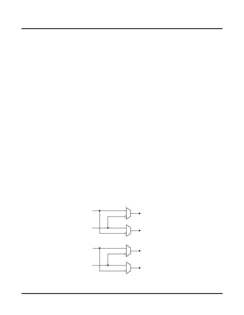
�GLB� Clock� Generator�
�Each� ispMACH� 4000� device� has� up� to� four� clock� pins� that� are� also� routed� to� the� GRP� to� be� used� as� inputs.� These�
�pins� drive� a� clock� generator� in� each� GLB,� as� shown� in� Figure� 6.� The� clock� generator� provides� four� clock� signals� that�
�can� be� used� anywhere� in� the� GLB.� These� four� GLB� clock� signals� can� consist� of� a� number� of� combinations� of� the�
�true� and� complement� edges� of� the� global� clock� signals.�
�Figure� 6.� GLB� Clock� Generator�
�CLK0�
�Block� CLK0�
�CLK1�
�Block� CLK1�
�CLK2�
�Block� CLK2�
�CLK3�
�8�
�Block� CLK3�
�相关PDF资料 |
PDF描述 |
|---|---|
| TAP474M035BRS | CAP TANT 0.47UF 35V 20% RADIAL |
| ASM22DTAN-S189 | CONN EDGECARD 44POS R/A .156 SLD |
| VE-23H-EV-F2 | CONVERTER MOD DC/DC 52V 150W |
| AGM22DTAN-S189 | CONN EDGECARD 44POS R/A .156 SLD |
| AYM22DTAH-S189 | CONN EDGECARD 44POS R/A .156 SLD |
相关代理商/技术参数 |
参数描述 |
|---|---|
| LC4032B-5T48C | 功能描述:CPLD - 复杂可编程逻辑器件 PROGRAMMABLE SUPER FAST HI DENSITY PLD RoHS:否 制造商:Lattice 系列: 存储类型:EEPROM 大电池数量:128 最大工作频率:333 MHz 延迟时间:2.7 ns 可编程输入/输出端数量:64 工作电源电压:3.3 V 最大工作温度:+ 90 C 最小工作温度:0 C 封装 / 箱体:TQFP-100 |
| LC4032B-5T48I | 功能描述:CPLD - 复杂可编程逻辑器件 PROGRAMMABLE SUPER FAST HI DENSITY PLD RoHS:否 制造商:Lattice 系列: 存储类型:EEPROM 大电池数量:128 最大工作频率:333 MHz 延迟时间:2.7 ns 可编程输入/输出端数量:64 工作电源电压:3.3 V 最大工作温度:+ 90 C 最小工作温度:0 C 封装 / 箱体:TQFP-100 |
| LC4032B-5TN44C | 功能描述:CPLD - 复杂可编程逻辑器件 PROGRAMMABLE SUPER FAST HI DENSITY PLD RoHS:否 制造商:Lattice 系列: 存储类型:EEPROM 大电池数量:128 最大工作频率:333 MHz 延迟时间:2.7 ns 可编程输入/输出端数量:64 工作电源电压:3.3 V 最大工作温度:+ 90 C 最小工作温度:0 C 封装 / 箱体:TQFP-100 |
| LC4032B-5TN44I | 功能描述:CPLD - 复杂可编程逻辑器件 PROGRAMMABLE SUPER FAST HI DENSITY PLD RoHS:否 制造商:Lattice 系列: 存储类型:EEPROM 大电池数量:128 最大工作频率:333 MHz 延迟时间:2.7 ns 可编程输入/输出端数量:64 工作电源电压:3.3 V 最大工作温度:+ 90 C 最小工作温度:0 C 封装 / 箱体:TQFP-100 |
| LC4032B-5TN48C | 功能描述:CPLD - 复杂可编程逻辑器件 PROGRAMMABLE SUPER FAST HI DENSITY PLD RoHS:否 制造商:Lattice 系列: 存储类型:EEPROM 大电池数量:128 最大工作频率:333 MHz 延迟时间:2.7 ns 可编程输入/输出端数量:64 工作电源电压:3.3 V 最大工作温度:+ 90 C 最小工作温度:0 C 封装 / 箱体:TQFP-100 |
发布紧急采购,3分钟左右您将得到回复。