- 您现在的位置:买卖IC网 > PDF目录22135 > LC4032ZC-35T48C (Lattice Semiconductor Corporation)IC PLD 32MC 32I/O 3.5NS 48TQFP PDF资料下载
参数资料
| 型号: | LC4032ZC-35T48C |
| 厂商: | Lattice Semiconductor Corporation |
| 文件页数: | 7/99页 |
| 文件大小: | 0K |
| 描述: | IC PLD 32MC 32I/O 3.5NS 48TQFP |
| 标准包装: | 250 |
| 系列: | ispMACH® 4000Z |
| 可编程类型: | 系统内可编程 |
| 最大延迟时间 tpd(1): | 3.5ns |
| 电压电源 - 内部: | 1.7 V ~ 1.9 V |
| 逻辑元件/逻辑块数目: | 2 |
| 宏单元数: | 32 |
| 输入/输出数: | 32 |
| 工作温度: | 0°C ~ 90°C |
| 安装类型: | 表面贴装 |
| 封装/外壳: | 48-LQFP |
| 供应商设备封装: | 48-TQFP(7x7) |
| 包装: | 托盘 |
第1页第2页第3页第4页第5页第6页当前第7页第8页第9页第10页第11页第12页第13页第14页第15页第16页第17页第18页第19页第20页第21页第22页第23页第24页第25页第26页第27页第28页第29页第30页第31页第32页第33页第34页第35页第36页第37页第38页第39页第40页第41页第42页第43页第44页第45页第46页第47页第48页第49页第50页第51页第52页第53页第54页第55页第56页第57页第58页第59页第60页第61页第62页第63页第64页第65页第66页第67页第68页第69页第70页第71页第72页第73页第74页第75页第76页第77页第78页第79页第80页第81页第82页第83页第84页第85页第86页第87页第88页第89页第90页第91页第92页第93页第94页第95页第96页第97页第98页第99页
�� �
�
�Lattice� Semiconductor�
�Table� 5.� Product� Term� Expansion� Capability�
�ispMACH� 4000V/B/C/Z� Family� Data� Sheet�
�Expansion�
�Chains�
�Chain-0�
�Chain-1�
�Chain-2�
�Chain-3�
�Macrocells� Associated� with� Expansion� Chain�
�(with� Wrap� Around)�
�M0� M4� M8� M12� M0�
�M1� M5� M9� M13� M1�
�M2� M6� M10� M14� M2�
�M3� M7� M11� M15� M3�
�Max� PT/�
�Macrocell�
�75�
�80�
�75�
�70�
�Every� time� the� super� cluster� allocator� is� used,� there� is� an� incremental� delay� of� t� EXP� .� When� the� super� cluster� alloca-�
�tor� is� used,� all� destinations� other� than� the� one� being� steered� to,� are� given� the� value� of� ground� (i.e.,� if� the� super� clus-�
�ter� is� steered� to� M� (n+4),� then� M� (n)� is� ground).�
�Macrocell�
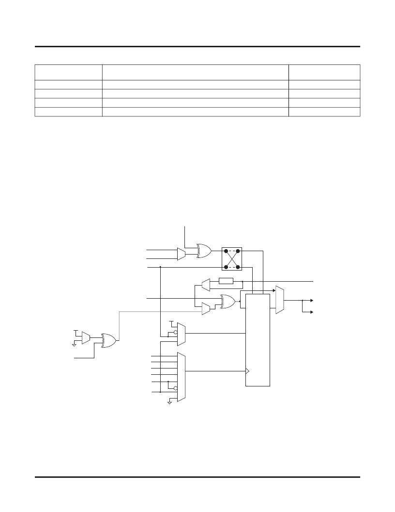
�The� 16� macrocells� in� the� GLB� are� driven� by� the� 16� outputs� from� the� logic� allocator.� Each� macrocell� contains� a� pro-�
�grammable� XOR� gate,� a� programmable� register/latch,� along� with� routing� for� the� logic� and� control� functions.�
�Figure� 5� shows� a� graphical� representation� of� the� macrocell.� The� macrocells� feed� the� ORP� and� GRP.� A� direct� input�
�from� the� I/O� cell� allows� designers� to� use� the� macrocell� to� construct� high-speed� input� registers.� A� programmable�
�delay� in� this� path� allows� designers� to� choose� between� the� fastest� possible� set-up� time� and� zero� hold� time.�
�Figure� 5.� Macrocell�
�Power-up�
�Initialization�
�Shared� PT� Initialization�
�PT� Initialization� (optional)�
�PT� Initialization/CE� (optional)�
�Delay�
�From� I/O� Cell�
�From� Logic� Allocator�
�R�
�D/T/L�
�P�
�Q�
�To� ORP�
�To� GRP�
�CE�
�Single� PT�
�Block� CLK0�
�Block� CLK1�
�Block� CLK2�
�Block� CLK3�
�PT� Clock� (optional)�
�Shared� PT� Clock�
�Enhanced� Clock� Multiplexer�
�The� clock� input� to� the� flip-flop� can� select� any� of� the� four� block� clocks� along� with� the� shared� PT� clock,� and� true� and�
�complement� forms� of� the� optional� individual� term� clock.� An� 8:1� multiplexer� structure� is� used� to� select� the� clock.� The�
�eight� sources� for� the� clock� multiplexer� are� as� follows:�
�?� Block� CLK0�
�?� Block� CLK1�
�7�
�相关PDF资料 |
PDF描述 |
|---|---|
| GRM188R71A105KA61D | CAP CER 1UF 10V 10% X7R 0603 |
| GBM24DCTD | CONN EDGECARD 48POS DIP .156 SLD |
| LC4032ZC-5TN48I | IC CPLD 32MACROCELLS 48TQFP |
| 7-530655-3 | CONN LOW PRO 12 POS 156X200C/L |
| EEM18DTAS | CONN EDGECARD 36POS R/A .156 SLD |
相关代理商/技术参数 |
参数描述 |
|---|---|
| LC4032ZC-35TN48C | 功能描述:CPLD - 复杂可编程逻辑器件 PROGRAMMABLE SUPER FAST HI DENSITY PLD RoHS:否 制造商:Lattice 系列: 存储类型:EEPROM 大电池数量:128 最大工作频率:333 MHz 延迟时间:2.7 ns 可编程输入/输出端数量:64 工作电源电压:3.3 V 最大工作温度:+ 90 C 最小工作温度:0 C 封装 / 箱体:TQFP-100 |
| LC4032ZC-5M56C | 功能描述:CPLD - 复杂可编程逻辑器件 PROGRAMMABLE SUPER FAST HI DENSITY PLD RoHS:否 制造商:Lattice 系列: 存储类型:EEPROM 大电池数量:128 最大工作频率:333 MHz 延迟时间:2.7 ns 可编程输入/输出端数量:64 工作电源电压:3.3 V 最大工作温度:+ 90 C 最小工作温度:0 C 封装 / 箱体:TQFP-100 |
| LC4032ZC-5M56I | 功能描述:CPLD - 复杂可编程逻辑器件 PROGRAMMABLE SUPER FAST HI DENSITY PLD RoHS:否 制造商:Lattice 系列: 存储类型:EEPROM 大电池数量:128 最大工作频率:333 MHz 延迟时间:2.7 ns 可编程输入/输出端数量:64 工作电源电压:3.3 V 最大工作温度:+ 90 C 最小工作温度:0 C 封装 / 箱体:TQFP-100 |
| LC4032ZC-5MN56C | 功能描述:CPLD - 复杂可编程逻辑器件 PROGRAMMABLE SUPER FAST HI DENSITY PLD RoHS:否 制造商:Lattice 系列: 存储类型:EEPROM 大电池数量:128 最大工作频率:333 MHz 延迟时间:2.7 ns 可编程输入/输出端数量:64 工作电源电压:3.3 V 最大工作温度:+ 90 C 最小工作温度:0 C 封装 / 箱体:TQFP-100 |
| LC4032ZC-5MN56I | 功能描述:CPLD - 复杂可编程逻辑器件 PROGRAMMABLE SUPER FAST HI DENSITY PLD RoHS:否 制造商:Lattice 系列: 存储类型:EEPROM 大电池数量:128 最大工作频率:333 MHz 延迟时间:2.7 ns 可编程输入/输出端数量:64 工作电源电压:3.3 V 最大工作温度:+ 90 C 最小工作温度:0 C 封装 / 箱体:TQFP-100 |
发布紧急采购,3分钟左右您将得到回复。