- 您现在的位置:买卖IC网 > PDF目录177655 > LC4256V-75F256AC (LATTICE SEMICONDUCTOR CORP) PDF资料下载
参数资料
| 型号: | LC4256V-75F256AC |
| 厂商: | LATTICE SEMICONDUCTOR CORP |
| 元件分类: | PLD |
| 中文描述: | EE PLD, 7.5 ns, PBGA256 |
| 封装: | FPBGA-256 |
| 文件页数: | 8/99页 |
| 文件大小: | 760K |
| 代理商: | LC4256V-75F256AC |
第1页第2页第3页第4页第5页第6页第7页当前第8页第9页第10页第11页第12页第13页第14页第15页第16页第17页第18页第19页第20页第21页第22页第23页第24页第25页第26页第27页第28页第29页第30页第31页第32页第33页第34页第35页第36页第37页第38页第39页第40页第41页第42页第43页第44页第45页第46页第47页第48页第49页第50页第51页第52页第53页第54页第55页第56页第57页第58页第59页第60页第61页第62页第63页第64页第65页第66页第67页第68页第69页第70页第71页第72页第73页第74页第75页第76页第77页第78页第79页第80页第81页第82页第83页第84页第85页第86页第87页第88页第89页第90页第91页第92页第93页第94页第95页第96页第97页第98页第99页
Lattice Semiconductor
ispMACH 4000V/B/C/Z Family Data Sheet
16
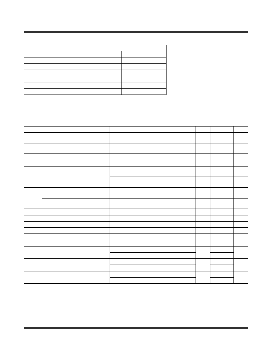
I/O Recommended Operating Conditions
DC Electrical Characteristics
Over Recommended Operating Conditions
Standard
VCCO (V)
1
Min.
Max.
LVTTL
3.0
3.6
LVCMOS 3.3
3.0
3.6
Extended LVCMOS 3.3
2
2.7
3.6
LVCMOS 2.5
2.3
2.7
LVCMOS 1.8
1.65
1.95
PCI 3.3
3.0
3.6
1. Typical values for VCCO are the average of the min. and max. values.
2. ispMACH 4000Z only.
Symbol
Parameter
Condition
Min.
Typ.
Max.
Units
IIL, IIH
1, 4
Input Leakage Current (ispMACH
4000Z)
0
V
IN < VCCO
—
0.51A
IIH
1
Input High Leakage Current (isp-
MACH 4000Z)
VCCO < VIN 5.5V
—
10
A
IIL, IIH
1
Input Leakage Current (ispMACH
4000V/B/C)
0
V
IN 3.6V, Tj = 105°C
—
10
A
0
V
IN 3.6V, Tj = 130°C
—
15
A
IIH
1,2
Input High Leakage Current (isp-
MACH 4000V/B/C)
3.6V < VIN 5.5V, Tj = 105°C
3.0V
V
CCO 3.6V
——
20
A
3.6V < VIN 5.5V, Tj = 130°C
3.0V
V
CCO 3.6V
——
50
A
IPU
I/O Weak Pull-up Resistor Current
(ispMACH 4000Z)
0
V
IN 0.7VCCO
-30
—
-150
A
I/O Weak Pull-up Resistor Current
(ispMACH 4000V/B/C)
0
V
IN 0.7VCCO
-30
—
-200
A
IPD
I/O Weak Pull-down Resistor Current VIL (MAX) VIN VIH (MIN)
30
—
150
A
IBHLS
Bus Hold Low Sustaining Current
VIN = VIL (MAX)
30
—
A
IBHHS
Bus Hold High Sustaining Current
VIN = 0.7 VCCO
-30
—
A
IBHLO
Bus Hold Low Overdrive Current
0V
V
IN VBHT
—
150
A
IBHHO
Bus Hold High Overdrive Current
VBHT VIN VCCO
——
-150
A
VBHT
Bus Hold Trip Points
—
VCCO * 0.35
—
VCCO * 0.65
V
C1
I/O Capacitance
3
VCCO = 3.3V, 2.5V, 1.8V
—
8
—
pf
VCC = 1.8V, VIO = 0 to VIH (MAX)
—
C2
Clock Capacitance
3
VCCO = 3.3V, 2.5V, 1.8V
—
6
—
pf
VCC = 1.8V, VIO = 0 to VIH (MAX)
—
C3
Global Input Capacitance
3
VCCO = 3.3V, 2.5V, 1.8V
—
6
—
pf
VCC = 1.8V, VIO = 0 to VIH (MAX)
—
1. Input or I/O leakage current is measured with the pin configured as an input or as an I/O with the output driver tristated. It is not
measured with the output driver active. Bus maintenance circuits are disabled.
2. 5V tolerant inputs and I/O should only be placed in banks where 3.0V
V
CCO 3.6V.
3. TA = 25°C, f = 1.0MHz
4. IIH excursions of up to 1.5A maximum per pin above the spec limit may be observed for certain voltage conditions on no more than 10% of
the device’s I/O pins.
相关PDF资料 |
PDF描述 |
|---|---|
| LC4064ZC-75T48I | |
| LC4032V-10T48I | |
| LC4512C-35F256C | |
| LC4512V-75F256I | |
| LC4256C-3FT256BC | |
相关代理商/技术参数 |
参数描述 |
|---|---|
| LC4256V-75F256AC1 | 制造商:LATTICE 制造商全称:Lattice Semiconductor 功能描述:3.3V/2.5V/1.8V In-System Programmable SuperFAST High Density PLDs |
| LC4256V-75F256AI | 功能描述:CPLD - 复杂可编程逻辑器件 PROGRAMMABLE SUPER FAST HI DENSITY PLD RoHS:否 制造商:Lattice 系列: 存储类型:EEPROM 大电池数量:128 最大工作频率:333 MHz 延迟时间:2.7 ns 可编程输入/输出端数量:64 工作电源电压:3.3 V 最大工作温度:+ 90 C 最小工作温度:0 C 封装 / 箱体:TQFP-100 |
| LC4256V-75F256AI1 | 制造商:LATTICE 制造商全称:Lattice Semiconductor 功能描述:3.3V/2.5V/1.8V In-System Programmable SuperFAST High Density PLDs |
| LC4256V-75F256B-10I | 制造商:Lattice Semiconductor Corporation 功能描述: |
| LC4256V-75F256BC | 功能描述:CPLD - 复杂可编程逻辑器件 3.3V 160 I/O RoHS:否 制造商:Lattice 系列: 存储类型:EEPROM 大电池数量:128 最大工作频率:333 MHz 延迟时间:2.7 ns 可编程输入/输出端数量:64 工作电源电压:3.3 V 最大工作温度:+ 90 C 最小工作温度:0 C 封装 / 箱体:TQFP-100 |
发布紧急采购,3分钟左右您将得到回复。