- 您现在的位置:买卖IC网 > PDF目录19656 > LC51024MV-75FN484C (Lattice Semiconductor Corporation)IC CPLD 1024MACROCELLS 484FPBGA PDF资料下载
参数资料
| 型号: | LC51024MV-75FN484C |
| 厂商: | Lattice Semiconductor Corporation |
| 文件页数: | 11/99页 |
| 文件大小: | 0K |
| 描述: | IC CPLD 1024MACROCELLS 484FPBGA |
| 标准包装: | 60 |
| 系列: | ispXPLD® 5000MV |
| 可编程类型: | 系统内可编程 |
| 最大延迟时间 tpd(1): | 7.5ns |
| 电压电源 - 内部: | 3 V ~ 3.6 V |
| 逻辑元件/逻辑块数目: | 32 |
| 宏单元数: | 1024 |
| 输入/输出数: | 317 |
| 工作温度: | 0°C ~ 90°C |
| 安装类型: | 表面贴装 |
| 封装/外壳: | 484-BBGA |
| 供应商设备封装: | 484-FPBGA(23x23) |
| 包装: | 托盘 |
第1页第2页第3页第4页第5页第6页第7页第8页第9页第10页当前第11页第12页第13页第14页第15页第16页第17页第18页第19页第20页第21页第22页第23页第24页第25页第26页第27页第28页第29页第30页第31页第32页第33页第34页第35页第36页第37页第38页第39页第40页第41页第42页第43页第44页第45页第46页第47页第48页第49页第50页第51页第52页第53页第54页第55页第56页第57页第58页第59页第60页第61页第62页第63页第64页第65页第66页第67页第68页第69页第70页第71页第72页第73页第74页第75页第76页第77页第78页第79页第80页第81页第82页第83页第84页第85页第86页第87页第88页第89页第90页第91页第92页第93页第94页第95页第96页第97页第98页第99页
Lattice Semiconductor
ispXPLD 5000MX Family Data Sheet
15
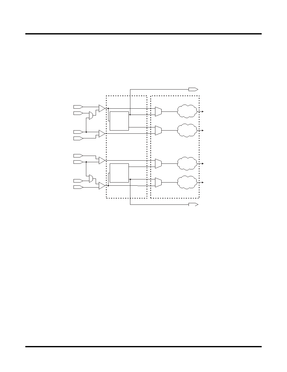
Clock Distribution
The ispXPLD 5000MX family has four dedicated clock input pins: GCLK0-GCLK3. GLCK0 and GCLK3 can be
routed through a PLL circuit or routed directly to the internal clock nets. The internal clock nets (CLK0-CLK3) are
directly related to the dedicated clock pins (see Secondary Clock Divider exception when using the sysCLOCK cir-
cuit). These feed the registers in the MFBs. Note at each register there is the option of inverting the clock if
required. Figure 14 shows the clock distribution network.
Figure 14. Clock Distribution Network
sysCLOCK PLL
The sysCLOCK PLL circuitry consists of Phase-Lock Loops (PLLs) and the various dividers, reset and feedback
signals associated with the PLLs. This feature gives the user the ability to synthesize clock frequencies and gener-
ate multiple clock signals for routing within the device. Furthermore, it can generate clock signals that are de-
skewed either at the board level or the device level.
The ispXPLD 5000MX devices provide two PLL circuits. PLL0 receives its clock inputs from GCLK 0 and provides
outputs to CLK 0 (CLK 1 when using the secondary clock). PLL1 operates with signals from GCLK 3 and CLK 3
(CLK 2 when using the secondary clock). The optional outputs CLK_OUT can be routed to an I/O pin. The optional
PLL_LOCK output is routed into the GRP. The optional input PLL_RST can be routed either from the GRP or
directly from an I/O pin. The optional PLL_FBK into can be routed directly from a pin. Figure 15 shows the ispXPLD
5000MX PLL block diagram. Figure 16 shows the connection of optional inputs and outputs.
sysCLOCK PLLs
Global Clock Routing
Clock Net
PLL0
CLK_OUT0
SEC_OUT0
VREF0
CLK0
CLK1
GCLK0
GCLK1
I/O/CLK_OUT0
Clock Net
PLL1
CLK_OUT1
SEC_OUT1
CLK3
CLK2
GCLK3
GCLK2
I/O/CLK_OUT1
Clock Net
To Macrocells
VREF1
VREF3
VREF2
SELECT
DEVICES
DISCONTINUED
相关PDF资料 |
PDF描述 |
|---|---|
| MIC5233-3.0BM5 TR | IC REG LDO 3V .1A SOT23-5 |
| ATF1508AS-10AC100 | IC CPLD 128 MACROCELL 100TQFP |
| RSM28DSAS | CONN EDGECARD 56POS R/A .156 SLD |
| GSC65DRES-S13 | CONN EDGECARD 130PS .100 EXTEND |
| ATF1504ASVL-20JC84 | IC CPLD 64MACROCELL LV LP 84PLCC |
相关代理商/技术参数 |
参数描述 |
|---|---|
| LC51024MV-75FN484I | 功能描述:CPLD - 复杂可编程逻辑器件 PROGRAM EXPANDED LOG RoHS:否 制造商:Lattice 系列: 存储类型:EEPROM 大电池数量:128 最大工作频率:333 MHz 延迟时间:2.7 ns 可编程输入/输出端数量:64 工作电源电压:3.3 V 最大工作温度:+ 90 C 最小工作温度:0 C 封装 / 箱体:TQFP-100 |
| LC51024MV-75FN672C | 功能描述:CPLD - 复杂可编程逻辑器件 PROGRAM EXPANDED LOG RoHS:否 制造商:Lattice 系列: 存储类型:EEPROM 大电池数量:128 最大工作频率:333 MHz 延迟时间:2.7 ns 可编程输入/输出端数量:64 工作电源电压:3.3 V 最大工作温度:+ 90 C 最小工作温度:0 C 封装 / 箱体:TQFP-100 |
| LC51024MV-75FN672I | 功能描述:CPLD - 复杂可编程逻辑器件 PROGRAM EXPANDED LOG RoHS:否 制造商:Lattice 系列: 存储类型:EEPROM 大电池数量:128 最大工作频率:333 MHz 延迟时间:2.7 ns 可编程输入/输出端数量:64 工作电源电压:3.3 V 最大工作温度:+ 90 C 最小工作温度:0 C 封装 / 箱体:TQFP-100 |
| LC51024MV-75Q208C | 制造商:LATTICE 制造商全称:Lattice Semiconductor 功能描述:3.3V, 2.5V and 1.8V In-System Programmable eXpanded Programmable Logic Device XPLD⑩ Family |
| LC51024MV-75Q208I | 制造商:LATTICE 制造商全称:Lattice Semiconductor 功能描述:3.3V, 2.5V and 1.8V In-System Programmable eXpanded Programmable Logic Device XPLD⑩ Family |
发布紧急采购,3分钟左右您将得到回复。