- 您现在的位置:买卖IC网 > PDF目录19591 > LC51024VG-75F676C (Lattice Semiconductor Corporation)IC XPLD 1024MC 7.5NS 676FPBGA PDF资料下载
参数资料
| 型号: | LC51024VG-75F676C |
| 厂商: | Lattice Semiconductor Corporation |
| 文件页数: | 5/99页 |
| 文件大小: | 0K |
| 描述: | IC XPLD 1024MC 7.5NS 676FPBGA |
| 标准包装: | 27 |
| 系列: | ispMACH™ 5000VG |
| 可编程类型: | 系统内可编程 |
| 最大延迟时间 tpd(1): | 7.5ns |
| 电压电源 - 内部: | 3 V ~ 3.6 V |
| 逻辑元件/逻辑块数目: | 32 |
| 宏单元数: | 1024 |
| 输入/输出数: | 384 |
| 工作温度: | 0°C ~ 90°C |
| 安装类型: | 表面贴装 |
| 封装/外壳: | 676-BBGA |
| 供应商设备封装: | 676-FPBGA(31x31) |
| 包装: | 托盘 |
第1页第2页第3页第4页当前第5页第6页第7页第8页第9页第10页第11页第12页第13页第14页第15页第16页第17页第18页第19页第20页第21页第22页第23页第24页第25页第26页第27页第28页第29页第30页第31页第32页第33页第34页第35页第36页第37页第38页第39页第40页第41页第42页第43页第44页第45页第46页第47页第48页第49页第50页第51页第52页第53页第54页第55页第56页第57页第58页第59页第60页第61页第62页第63页第64页第65页第66页第67页第68页第69页第70页第71页第72页第73页第74页第75页第76页第77页第78页第79页第80页第81页第82页第83页第84页第85页第86页第87页第88页第89页第90页第91页第92页第93页第94页第95页第96页第97页第98页第99页
Lattice Semiconductor
ispXPLD 5000MX Family Data Sheet
9
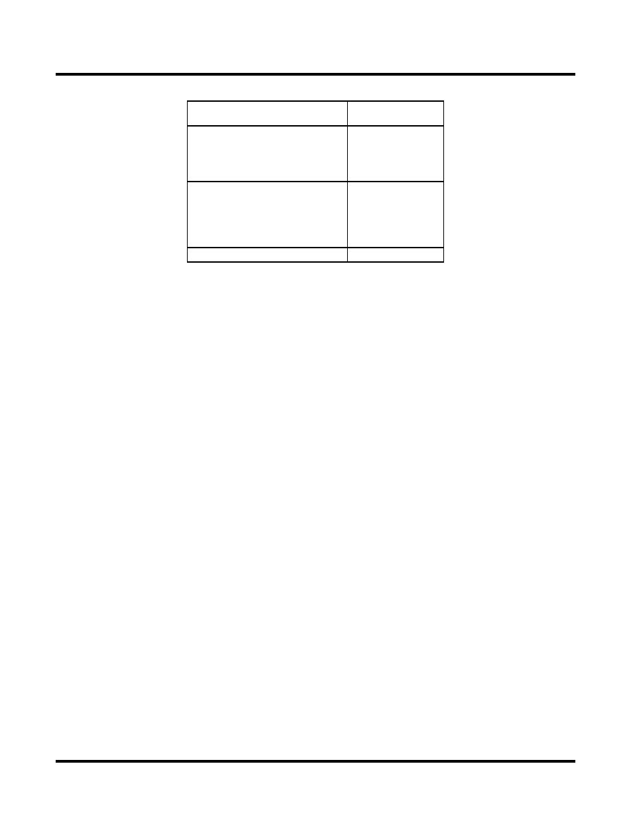
Table 4. MFB Memory Configuration
Input and Output
The data input and control signals to a MFB in memory mode are generated from inputs from the routing. Data sig-
nals are only available in the true non-inverted format. True or complemented versions of the inputs are available
for generating the control signals. Data and flag outputs are fed from the MFB to the GRP and OSA. Unused inputs
and outputs are not accessible in memory mode.
ROM Operation
In each of the memory modes it is possible to specify the power-on state of each bit in the memory array. This
allows the memory to be used as ROM if desired.
Increased Depth And Width
Designs that require a memory depth or width that is greater than that support by a single MFB can be supported
by cascading multiple blocks. For dual port, single port, and pseudo dual port modes additional width is easily pro-
vided by sharing address lines. Additional depth is supported by multiplexing the RAM output. For FIFO and CAM
modes additional width is supported through the cascading of MFBs.
The Lattice design tools automatically combine blocks to support the memory size specified in the user’s design.
Bus Size Matching
All of the memory modes apart from CAM mode support different widths on each of the ports. The RAM bits are
mapped LSB word 0 to MSB word 0, LSB word 1 to MSB word 1 and so on. Although the word size and number of
words for each port varies this mapping scheme applies to each port.
Memory Mode
Max. Configuration
Size
1
Dual-port
8,192 x 1
4,096 x 2
2,048 x 4
1,024 x 8
512 x 16
Single-port, Pseudo Dual Port, FIFO
16,384 x1
8,192 x 2
4,096 x 4
2,048 x 8
1,024 x 16
512 x 32
CAM
128 x 48
1. Smaller configurations are possible.
SELECT
DEVICES
DISCONTINUED
相关PDF资料 |
PDF描述 |
|---|---|
| RMC31DRAI-S734 | CONN EDGECARD 62POS .100 R/A PCB |
| VE-B5M-CX-B1 | CONVERTER MOD DC/DC 10V 75W |
| ECC08DCSH | CONN EDGECARD 16POS DIP .100 SLD |
| NCP1012AP100 | IC OFFLINE SWIT SMPS CM OVP 8DIP |
| PQ1U201M2ZPH | IC REG LDO 2V .15A SOT-23-5 |
相关代理商/技术参数 |
参数描述 |
|---|---|
| LC51024VG-75F676I | 功能描述:CPLD - 复杂可编程逻辑器件 PROGRAM EXPANDED LOG RoHS:否 制造商:Lattice 系列: 存储类型:EEPROM 大电池数量:128 最大工作频率:333 MHz 延迟时间:2.7 ns 可编程输入/输出端数量:64 工作电源电压:3.3 V 最大工作温度:+ 90 C 最小工作温度:0 C 封装 / 箱体:TQFP-100 |
| LC511 | 制造商:SEOUL 制造商全称:Seoul Semiconductor 功能描述:RED OVAL LAMP LED |
| LC511-200/N | 制造商:Newport Electronics Inc 功能描述:SENSOR, LOAD CELL, 200LB, 3MV/V, Load Capacity:200lb, Cell Output mV / V:3, External Depth:25mm, Length:121mm, Operating Temperature Min:-34C, Operating Temperature Max:82C, Supply Voltage:15VDC , RoHS Compliant: Yes |
| LC5128B-10T128I | 功能描述:CPLD - 复杂可编程逻辑器件 RoHS:否 制造商:Lattice 系列: 存储类型:EEPROM 大电池数量:128 最大工作频率:333 MHz 延迟时间:2.7 ns 可编程输入/输出端数量:64 工作电源电压:3.3 V 最大工作温度:+ 90 C 最小工作温度:0 C 封装 / 箱体:TQFP-100 |
| LC5128B-3T128C | 功能描述:CPLD - 复杂可编程逻辑器件 PROGRAM EXPANDED LOG RoHS:否 制造商:Lattice 系列: 存储类型:EEPROM 大电池数量:128 最大工作频率:333 MHz 延迟时间:2.7 ns 可编程输入/输出端数量:64 工作电源电压:3.3 V 最大工作温度:+ 90 C 最小工作温度:0 C 封装 / 箱体:TQFP-100 |
发布紧急采购,3分钟左右您将得到回复。