- 您现在的位置:买卖IC网 > PDF目录177665 > LC5512MC-75FN256I (LATTICE SEMICONDUCTOR CORP) PDF资料下载
参数资料
| 型号: | LC5512MC-75FN256I |
| 厂商: | LATTICE SEMICONDUCTOR CORP |
| 元件分类: | PLD |
| 中文描述: | EE PLD, 9.5 ns, PBGA256 |
| 封装: | LEAD FREE, FPBGA-256 |
| 文件页数: | 78/95页 |
| 文件大小: | 923K |
| 代理商: | LC5512MC-75FN256I |
第1页第2页第3页第4页第5页第6页第7页第8页第9页第10页第11页第12页第13页第14页第15页第16页第17页第18页第19页第20页第21页第22页第23页第24页第25页第26页第27页第28页第29页第30页第31页第32页第33页第34页第35页第36页第37页第38页第39页第40页第41页第42页第43页第44页第45页第46页第47页第48页第49页第50页第51页第52页第53页第54页第55页第56页第57页第58页第59页第60页第61页第62页第63页第64页第65页第66页第67页第68页第69页第70页第71页第72页第73页第74页第75页第76页第77页当前第78页第79页第80页第81页第82页第83页第84页第85页第86页第87页第88页第89页第90页第91页第92页第93页第94页第95页
Lattice Semiconductor
ispXPLD 5000MX Family Data Sheet
8
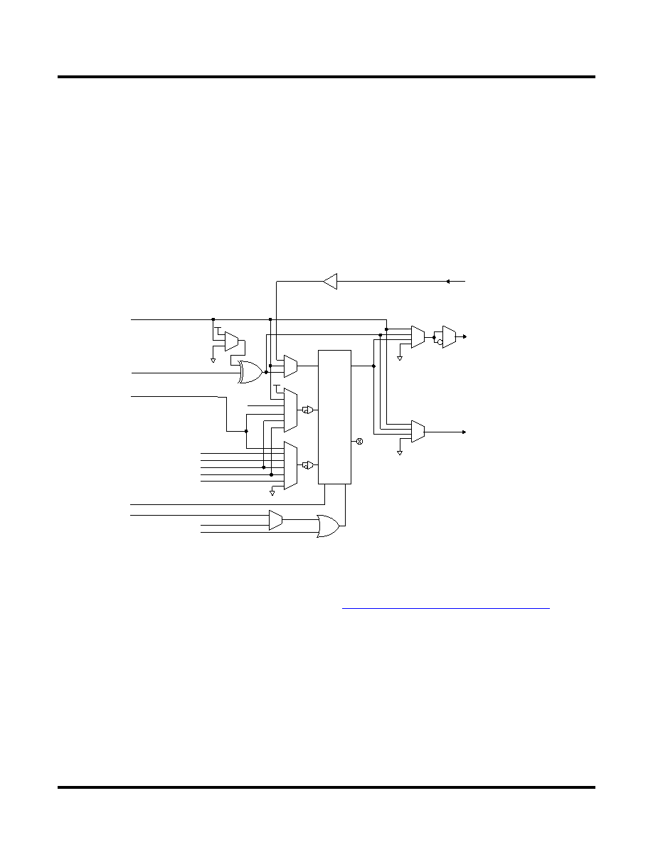
Macrocell
The 32 registered macrocells in the MFB are driven by the 32 outputs from the PTSA or the PTSA bypass. Each
macrocell contains a programmable XOR gate, a programmable register/latch flip-flop and the necessary clocks
and control logic to allow combinatorial or registered operation. All macrocells have an output that feeds the GRP.
Selected macrocells have an additional output that feeds the OSA and hence I/Os. This dual or concurrent output
capability from the macrocell gives efficient use of the hardware resources. One output can be a registered function
for example, while the other output can be an unrelated combinatorial function. A direct register input from the I/O
cell facilitates efficient use of the macrocell to construct high-speed input registers. Macrocell registers can be
clocked from one of several global or product term clocks available on the device. A global and product term clock
enable is also provided, eliminating the need to gate the clock to the macrocell registers directly. Reset and preset
for the macrocell register is provided from both global and product term signals. The macrocell register can be pro-
grammed to operate as a D-type register or a D-type latch. Figure 8 is a graphical representation of the macrocell.
Figure 8. Macrocell
Memory Modes
The ispXPLD 5000MX architecture allows the MFB to be configured as a variety of memory blocks as detailed in
Table 4. The remainder of this section details operation of each of the memory modes. Additional information
regarding the memory modes can also be found in TN1030, Using Memory in ispXPLD 5000MX Devices.
PTSA Bypass
From
I/O Cell
Output to
I/O Block
GRP
PT Clock
From PTSA
PT Preset
PT Reset
Shared PT Reset
Shared
PT CE
CLK0
CLK1
Shared PT Clock
CLK2
CLK3
Global Reset
Clk En
Clk
R/L
D
PR
Q
相关PDF资料 |
PDF描述 |
|---|---|
| LC51024MB-52FN672C | |
| LC5768MB-5FN484C | |
| LC5512MC-75FN256C | |
| LC51024MC-52FN672C | |
| LC5768MB-75FN256C | |
相关代理商/技术参数 |
参数描述 |
|---|---|
| LC5512MC-75FN484C | 功能描述:CPLD - 复杂可编程逻辑器件 PROGRAM EXPANDED LOG RoHS:否 制造商:Lattice 系列: 存储类型:EEPROM 大电池数量:128 最大工作频率:333 MHz 延迟时间:2.7 ns 可编程输入/输出端数量:64 工作电源电压:3.3 V 最大工作温度:+ 90 C 最小工作温度:0 C 封装 / 箱体:TQFP-100 |
| LC5512MC-75FN484I | 功能描述:CPLD - 复杂可编程逻辑器件 PROGRAM EXPANDED LOG RoHS:否 制造商:Lattice 系列: 存储类型:EEPROM 大电池数量:128 最大工作频率:333 MHz 延迟时间:2.7 ns 可编程输入/输出端数量:64 工作电源电压:3.3 V 最大工作温度:+ 90 C 最小工作温度:0 C 封装 / 箱体:TQFP-100 |
| LC5512MC-75FN672C | 制造商:LATTICE 制造商全称:Lattice Semiconductor 功能描述:3.3V, 2.5V and 1.8V In-System Programmable eXpanded Programmable Logic Device XPLD⑩ Family |
| LC5512MC-75FN672I | 制造商:LATTICE 制造商全称:Lattice Semiconductor 功能描述:3.3V, 2.5V and 1.8V In-System Programmable eXpanded Programmable Logic Device XPLD⑩ Family |
| LC5512MC-75Q208C | 功能描述:CPLD - 复杂可编程逻辑器件 PROGRAM EXPANDED LOG RoHS:否 制造商:Lattice 系列: 存储类型:EEPROM 大电池数量:128 最大工作频率:333 MHz 延迟时间:2.7 ns 可编程输入/输出端数量:64 工作电源电压:3.3 V 最大工作温度:+ 90 C 最小工作温度:0 C 封装 / 箱体:TQFP-100 |
发布紧急采购,3分钟左右您将得到回复。