- 您现在的位置:买卖IC网 > PDF目录177666 > LC5512MC-75FN484C (LATTICE SEMICONDUCTOR CORP) PDF资料下载
参数资料
| 型号: | LC5512MC-75FN484C |
| 厂商: | LATTICE SEMICONDUCTOR CORP |
| 元件分类: | PLD |
| 中文描述: | EE PLD, 9.5 ns, PBGA484 |
| 封装: | LEAD FREE, FPBGA-484 |
| 文件页数: | 11/95页 |
| 文件大小: | 923K |
| 代理商: | LC5512MC-75FN484C |
第1页第2页第3页第4页第5页第6页第7页第8页第9页第10页当前第11页第12页第13页第14页第15页第16页第17页第18页第19页第20页第21页第22页第23页第24页第25页第26页第27页第28页第29页第30页第31页第32页第33页第34页第35页第36页第37页第38页第39页第40页第41页第42页第43页第44页第45页第46页第47页第48页第49页第50页第51页第52页第53页第54页第55页第56页第57页第58页第59页第60页第61页第62页第63页第64页第65页第66页第67页第68页第69页第70页第71页第72页第73页第74页第75页第76页第77页第78页第79页第80页第81页第82页第83页第84页第85页第86页第87页第88页第89页第90页第91页第92页第93页第94页第95页
Lattice Semiconductor
ispXPLD 5000MX Family Data Sheet
19
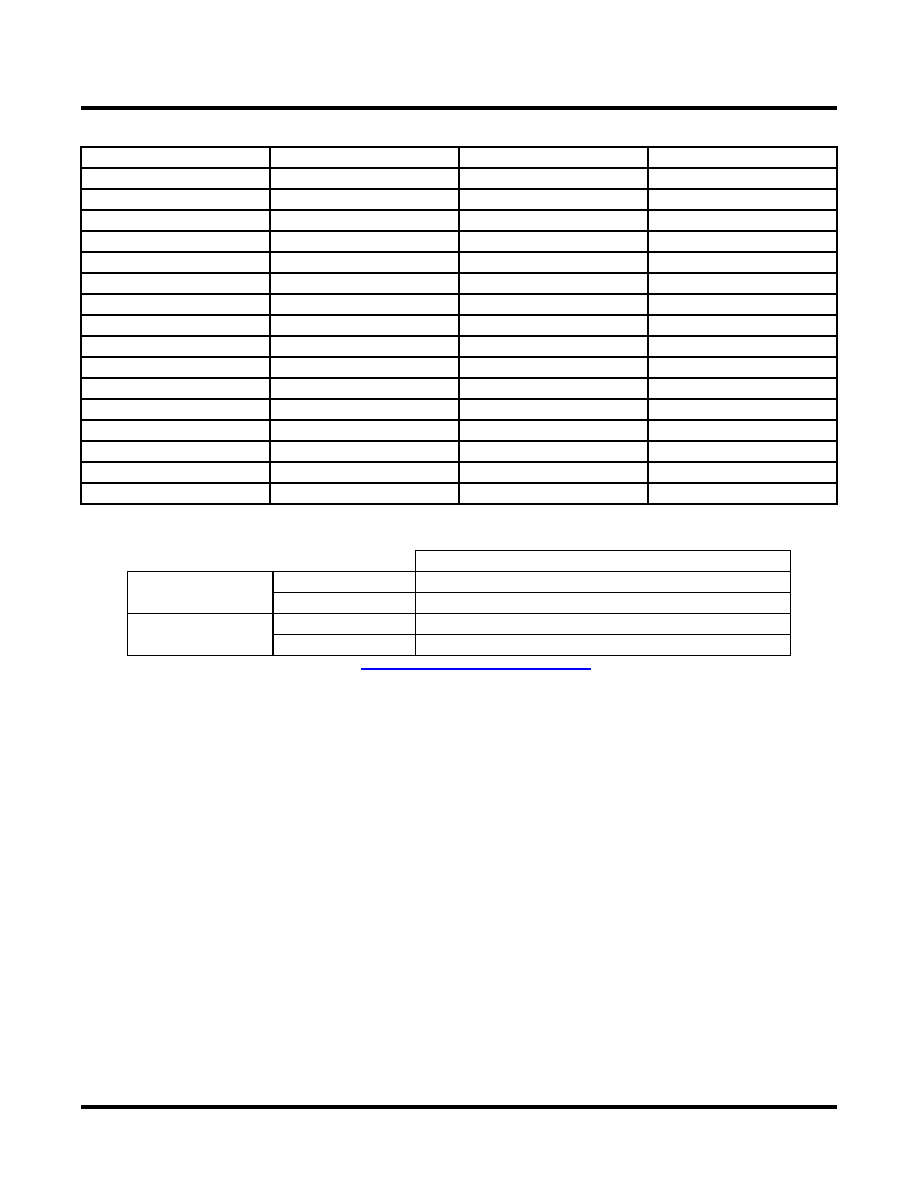
Table 12. ispXPLD 5000MX Supported I/O Standards
Table 13. Differential Interface Standard Support
1
Control, Clock, sysCONFIG and JTAG Signals
Global clock pins support the same sysIO standards as general purpose I/O. When required the VREF signal is
derived from the adjacent bank. When differential standards are supported two adjacent clock pins are paired to
form the input. The TOE, PROGRAM, CFG0 and DONE pins of the ispXPLD 5000MX device are the only pins that
do not have sysIO capabilities. The JTAG TAP pins support only LVCMOS 3.3, 2.5 and 1.8V standards. The voltage
is controlled by VCCJ. These pins only support the LVTTL and LVCMOS standards applicable to the power supply
voltage of the device. The global reset global output enable pins are associated with Bank 2 and support all of the
sysIO standards.
Hotsocketing
The I/O on the ispXPLD 5000MX devices are well suited for those applications that require hot socketing capability,
when configured as LVCMOS or LVTTL. Hot socketing a device requires that the device, when powered down, can
tolerate active signals on the I/Os and inputs without being damaged. Additionally, it requires that the effects of the
powered-down device be minimal on active signals.
Programmable Drive Strength
The drive strength of I/Os that are programmed as LVCMOS is tightly controlled and can be programmed to a vari-
ety of different values. Thus the impedance an output driver can be closely match to the characteristic impedance
of the line it is driving. This allows users to eliminate the need for external series termination resistors.
sysIO Standard
Nominal VCCO
Nominal VREF
Nominal VTT
LVTTL
3.3V
N/A
LVCMOS-3.3
3.3V
N/A
LVCMOS-2.5
2.5V
N/A
LVCMOS-1.8
1.8V
N/A
PCI 3.3V
3.3V
N/A
AGP-1X
3.3V
N/A
SSTL3, Class I & II
3.3V
1.5V
SSTL2, Class I & II
2.5V
1.25V
CTT 3.3
3.3V
1.5V
CTT 2.5
2.5V
1.25V
HSTL, Class I
1.5V
0.75V
HSTL, Class III
1.5V
0.9V
0.75V
HSTL, Class IV
1.5V
0.9V
0.75V
GTL+
N/A
1.0V
1.5V
LVPECL, Differential
2.5V, 3.3V
N/A
LVDS
2.5V, 3.3V
N/A
sysIO Buffer
LVDS
Driver
Supported
Receiver
Supported with standard termination
LVPECL
Driver
Supported with external resistor network
Receiver
Supported with termination
1. For more information, refer to TN1000 – sysIO Usage Guidelines for Lattice Devices.
相关PDF资料 |
PDF描述 |
|---|---|
| LC5256MC-5FN256C | |
| LC51024MB-52FN484C | |
| LC5512MB-75FN484C | |
| LC5512MC-75QN208C | |
| LC51024MB-75F484C | |
相关代理商/技术参数 |
参数描述 |
|---|---|
| LC5512MC-75FN484I | 功能描述:CPLD - 复杂可编程逻辑器件 PROGRAM EXPANDED LOG RoHS:否 制造商:Lattice 系列: 存储类型:EEPROM 大电池数量:128 最大工作频率:333 MHz 延迟时间:2.7 ns 可编程输入/输出端数量:64 工作电源电压:3.3 V 最大工作温度:+ 90 C 最小工作温度:0 C 封装 / 箱体:TQFP-100 |
| LC5512MC-75FN672C | 制造商:LATTICE 制造商全称:Lattice Semiconductor 功能描述:3.3V, 2.5V and 1.8V In-System Programmable eXpanded Programmable Logic Device XPLD⑩ Family |
| LC5512MC-75FN672I | 制造商:LATTICE 制造商全称:Lattice Semiconductor 功能描述:3.3V, 2.5V and 1.8V In-System Programmable eXpanded Programmable Logic Device XPLD⑩ Family |
| LC5512MC-75Q208C | 功能描述:CPLD - 复杂可编程逻辑器件 PROGRAM EXPANDED LOG RoHS:否 制造商:Lattice 系列: 存储类型:EEPROM 大电池数量:128 最大工作频率:333 MHz 延迟时间:2.7 ns 可编程输入/输出端数量:64 工作电源电压:3.3 V 最大工作温度:+ 90 C 最小工作温度:0 C 封装 / 箱体:TQFP-100 |
| LC5512MC-75Q208I | 功能描述:CPLD - 复杂可编程逻辑器件 PROGRAM EXPANDED LOG RoHS:否 制造商:Lattice 系列: 存储类型:EEPROM 大电池数量:128 最大工作频率:333 MHz 延迟时间:2.7 ns 可编程输入/输出端数量:64 工作电源电压:3.3 V 最大工作温度:+ 90 C 最小工作温度:0 C 封装 / 箱体:TQFP-100 |
发布紧急采购,3分钟左右您将得到回复。