- 您现在的位置:买卖IC网 > PDF目录19716 > LC5512MV-45FN256C (Lattice Semiconductor Corporation)IC CPLD 512MACROCELLS 256FPBGA PDF资料下载
参数资料
| 型号: | LC5512MV-45FN256C |
| 厂商: | Lattice Semiconductor Corporation |
| 文件页数: | 56/99页 |
| 文件大小: | 0K |
| 描述: | IC CPLD 512MACROCELLS 256FPBGA |
| 标准包装: | 90 |
| 系列: | ispXPLD® 5000MV |
| 可编程类型: | 系统内可编程 |
| 最大延迟时间 tpd(1): | 4.5ns |
| 电压电源 - 内部: | 3 V ~ 3.6 V |
| 逻辑元件/逻辑块数目: | 16 |
| 宏单元数: | 512 |
| 输入/输出数: | 193 |
| 工作温度: | 0°C ~ 90°C |
| 安装类型: | 表面贴装 |
| 封装/外壳: | 256-BGA |
| 供应商设备封装: | 256-FPBGA(17x17) |
| 包装: | 托盘 |
| 其它名称: | 220-1725 LC5512MV-45FN256C-ND |
第1页第2页第3页第4页第5页第6页第7页第8页第9页第10页第11页第12页第13页第14页第15页第16页第17页第18页第19页第20页第21页第22页第23页第24页第25页第26页第27页第28页第29页第30页第31页第32页第33页第34页第35页第36页第37页第38页第39页第40页第41页第42页第43页第44页第45页第46页第47页第48页第49页第50页第51页第52页第53页第54页第55页当前第56页第57页第58页第59页第60页第61页第62页第63页第64页第65页第66页第67页第68页第69页第70页第71页第72页第73页第74页第75页第76页第77页第78页第79页第80页第81页第82页第83页第84页第85页第86页第87页第88页第89页第90页第91页第92页第93页第94页第95页第96页第97页第98页第99页
Lattice Semiconductor
ispXPLD 5000MX Family Data Sheet
2
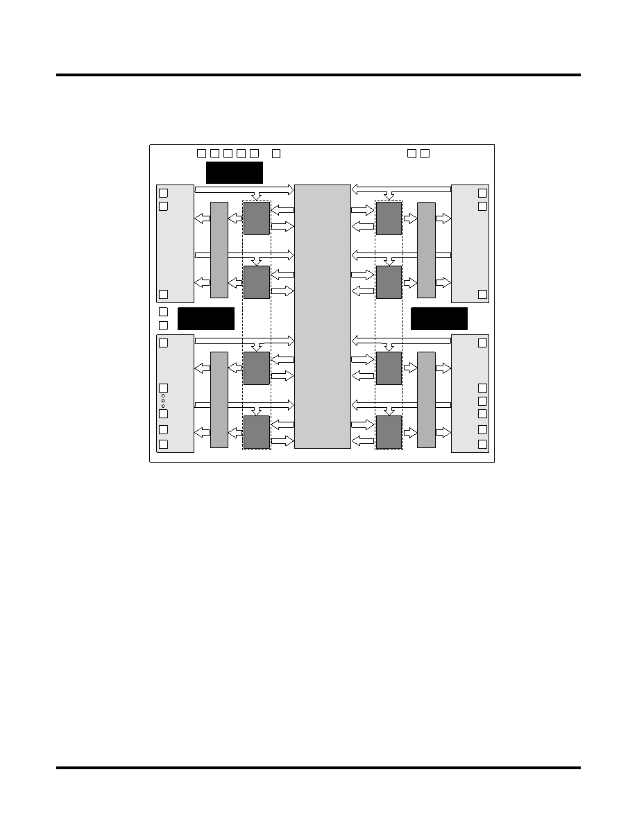
Figure 1. ispXPLD 5000MX Block Diagram
Introduction
The ispXPLD 5000MX family represents a new class of device, referred to as the eXpanded Programmable Logic
Devices (XPLDs). These devices extend the capability of Lattice’s popular SuperWIDE ispMACH 5000 architecture
by providing flexible memory capability. The family supports single- or dual-port SRAM, FIFO, and ternary CAM
operation. Extra logic has also been included to allow efficient implementation of arithmetic functions. In addition,
sysCLOCK PLLs and sysIO interfaces provide support for the system-level needs of designers.
The devices provide designers with a convenient one-chip solution that provides logic availability at boot-up, design
security, and extreme reconfigurability. The use of advanced process technology provides industry-leading perfor-
mance with combinatorial propagation delay as low as 4.0ns, 2.8ns clock-to-out delay, 2.2ns set-up time, and oper-
ating frequency up to 300MHz. This performance is coupled with low static and dynamic power consumption. The
ispXPLD 5000MX architecture provides predictable deterministic timing.
The availability of 3.3, 2.5 and 1.8V versions of these devices along with the flexibility of the sysIO interface helps
users meet the challenge of today’s mixed voltage designs. Inputs can be safely driven up to 5.5V when an I/O
bank is configured for 3.3V operation, making this family 5V tolerant. Boundary scan testability further eases inte-
gration into today’s complex systems. A variety of density and package options increase the likelihood of a good fit
for a particular application. Table 1 shows the members of the ispXPLD 5000MX family.
Architecture
The ispXPLD 5000MX devices consist of Multi-Function Blocks (MFBs) interconnected with a Global Routing Pool.
Signals enter and leave the device via one of four sysIO banks. Figure 1 shows the block diagram of the ispXPLD
ISP Port
Global
Routing
Pool
(GRP)
sysCLOCK
PLL 0
sysCLOCK
PLL 1
sysIO
Bank 0
MFB
VCCO3
V
CC
VREF3
VREF2
VCCO2
GCLCK3
GCLK2
RESET
GOE0
GOE1
TDO
GND
TDI
TMS
TCK
PROGRAM
OSA
sysIO
Bank 1
sysIO
Bank 3
sysIO
Bank 2
MFB
OSA
VCCO0
VCCO1
VCCP
VREF0
VREF1
GCLCK0
GNDP
GCLK1
Optional
sysCONFIG
Interface
V
CCJ
SELECT
DEVICES
DISCONTINUED
相关PDF资料 |
PDF描述 |
|---|---|
| MIC39151-2.5BU | IC REG LDO 2.5V 1.5A TO263-5 |
| GCM02DSXN | CONN EDGECARD 4POS DIP .156 SLD |
| LC5512MV-75Q208C | IC XPLD 512MC 7.5NS 208PQFP |
| 172-E09-102R021 | CONN DB9 MALE SOLDER CUP TIN |
| LC5512MC-75QN208C | IC XPLD 512MC 7.5NS 208PQFP |
相关代理商/技术参数 |
参数描述 |
|---|---|
| LC5512MV-45FN256I | 制造商:LATTICE 制造商全称:Lattice Semiconductor 功能描述:3.3V, 2.5V and 1.8V In-System Programmable eXpanded Programmable Logic Device XPLD⑩ Family |
| LC5512MV-45FN484C | 功能描述:CPLD - 复杂可编程逻辑器件 PROGRAM EXPANDED LOG RoHS:否 制造商:Lattice 系列: 存储类型:EEPROM 大电池数量:128 最大工作频率:333 MHz 延迟时间:2.7 ns 可编程输入/输出端数量:64 工作电源电压:3.3 V 最大工作温度:+ 90 C 最小工作温度:0 C 封装 / 箱体:TQFP-100 |
| LC5512MV-45FN484I | 制造商:LATTICE 制造商全称:Lattice Semiconductor 功能描述:3.3V, 2.5V and 1.8V In-System Programmable eXpanded Programmable Logic Device XPLD⑩ Family |
| LC5512MV-45FN672C | 制造商:LATTICE 制造商全称:Lattice Semiconductor 功能描述:3.3V, 2.5V and 1.8V In-System Programmable eXpanded Programmable Logic Device XPLD⑩ Family |
| LC5512MV-45FN672I | 制造商:LATTICE 制造商全称:Lattice Semiconductor 功能描述:3.3V, 2.5V and 1.8V In-System Programmable eXpanded Programmable Logic Device XPLD⑩ Family |
发布紧急采购,3分钟左右您将得到回复。