- 您现在的位置:买卖IC网 > PDF目录19687 > LC5768MV-75FN256C (Lattice Semiconductor Corporation)IC CPLD 512MACROCELLS 256FPBGA PDF资料下载
参数资料
| 型号: | LC5768MV-75FN256C |
| 厂商: | Lattice Semiconductor Corporation |
| 文件页数: | 13/99页 |
| 文件大小: | 0K |
| 描述: | IC CPLD 512MACROCELLS 256FPBGA |
| 标准包装: | 90 |
| 系列: | ispXPLD® 5000MV |
| 可编程类型: | 系统内可编程 |
| 最大延迟时间 tpd(1): | 7.5ns |
| 电压电源 - 内部: | 3 V ~ 3.6 V |
| 逻辑元件/逻辑块数目: | 24 |
| 宏单元数: | 768 |
| 输入/输出数: | 193 |
| 工作温度: | 0°C ~ 90°C |
| 安装类型: | 表面贴装 |
| 封装/外壳: | 256-BGA |
| 供应商设备封装: | 256-FPBGA(17x17) |
| 包装: | 托盘 |
第1页第2页第3页第4页第5页第6页第7页第8页第9页第10页第11页第12页当前第13页第14页第15页第16页第17页第18页第19页第20页第21页第22页第23页第24页第25页第26页第27页第28页第29页第30页第31页第32页第33页第34页第35页第36页第37页第38页第39页第40页第41页第42页第43页第44页第45页第46页第47页第48页第49页第50页第51页第52页第53页第54页第55页第56页第57页第58页第59页第60页第61页第62页第63页第64页第65页第66页第67页第68页第69页第70页第71页第72页第73页第74页第75页第76页第77页第78页第79页第80页第81页第82页第83页第84页第85页第86页第87页第88页第89页第90页第91页第92页第93页第94页第95页第96页第97页第98页第99页
Lattice Semiconductor
ispXPLD 5000MX Family Data Sheet
16
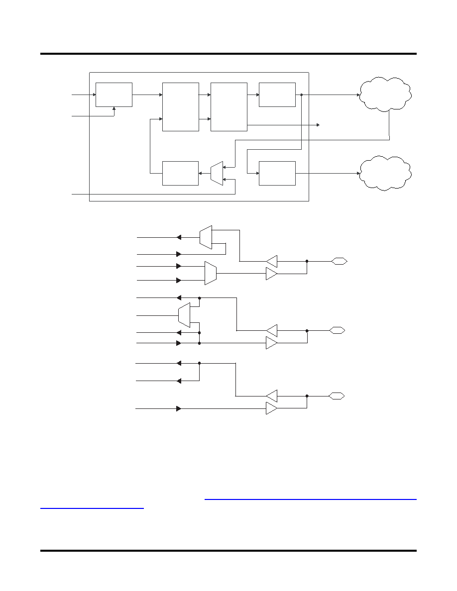
Figure 15. PLL Block Diagram
Figure 16. Connection of Optional PLL Inputs and Outputs
In order to facilitate the multiply and divide capabilities of the PLL, each PLL has dividers associated with it: M, N
and K. The M divider is used to divide the clock signal, while the N divider is used to multiply the clock signal. The
K divider is only used when a secondary clock output is needed. This divider divides the primary clock output and
feeds to a separate global clock net. The V divider is used to provide lower frequency output clocks, while maintain-
ing a stable, high frequency output from the PLL’s VCO circuit. The PLL also has a delay feature that allows the out-
put clock to be advanced or delayed to improve set-up and clock-to-out times for better performance. For more
information on the PLL, please refer to TN1003, sysCLOCK PLL Usage Guide for ispXPGA, ispGDX2, ispXPLD
SEC_OUT
CLK_OUT
PLL_LOCK
CLK_IN
PLL_RST
PLL_FBK
Input Clock
(M) Divider
Post-scalar
(V) Divider
VCO
and
Phase
Detector
Programable
Delay
Secondary
Clock
(K) Divider
Feedback
Loop
(N) Divider
Clock Net
PLL_LOCK
To GRP
CLK_OUT
From Macrocell
To GRP
PLL_RST
From Macrocell
To GRP
PLL_FBK
From Macrocell
I/O Pin*
*See pinout table for details
SELECT
DEVICES
DISCONTINUED
相关PDF资料 |
PDF描述 |
|---|---|
| MIC5206-5.0BMM | IC REG LDO 5V .15A 8-MSOP |
| M4A5-256/128-12YI | IC CPLD ISP 4A 256MC 208PQFP |
| OKL-T/3-W12N-C | CONV DC/DC 15W 12VIN 3AOUT SMD |
| M4A5-256/128-10YC | IC CPLD ISP 4A 256MC 208PQFP |
| GRM43DR73A473KW01L | CAP CER 0.047UF 1KV 10% X7R 1812 |
相关代理商/技术参数 |
参数描述 |
|---|---|
| LC5768MV-75FN256I | 功能描述:CPLD - 复杂可编程逻辑器件 PROGRAM EXPANDED LOG RoHS:否 制造商:Lattice 系列: 存储类型:EEPROM 大电池数量:128 最大工作频率:333 MHz 延迟时间:2.7 ns 可编程输入/输出端数量:64 工作电源电压:3.3 V 最大工作温度:+ 90 C 最小工作温度:0 C 封装 / 箱体:TQFP-100 |
| LC5768MV-75FN484C | 功能描述:CPLD - 复杂可编程逻辑器件 PROGRAM EXPANDED LOG RoHS:否 制造商:Lattice 系列: 存储类型:EEPROM 大电池数量:128 最大工作频率:333 MHz 延迟时间:2.7 ns 可编程输入/输出端数量:64 工作电源电压:3.3 V 最大工作温度:+ 90 C 最小工作温度:0 C 封装 / 箱体:TQFP-100 |
| LC5768MV-75FN484I | 功能描述:CPLD - 复杂可编程逻辑器件 PROGRAM EXPANDED LOG RoHS:否 制造商:Lattice 系列: 存储类型:EEPROM 大电池数量:128 最大工作频率:333 MHz 延迟时间:2.7 ns 可编程输入/输出端数量:64 工作电源电压:3.3 V 最大工作温度:+ 90 C 最小工作温度:0 C 封装 / 箱体:TQFP-100 |
| LC5768MV-75FN672C | 制造商:LATTICE 制造商全称:Lattice Semiconductor 功能描述:3.3V, 2.5V and 1.8V In-System Programmable eXpanded Programmable Logic Device XPLD⑩ Family |
| LC5768MV-75FN672I | 制造商:LATTICE 制造商全称:Lattice Semiconductor 功能描述:3.3V, 2.5V and 1.8V In-System Programmable eXpanded Programmable Logic Device XPLD⑩ Family |
发布紧急采购,3分钟左右您将得到回复。