- 您现在的位置:买卖IC网 > PDF目录30731 > LC72711LW (SANYO SEMICONDUCTOR CO LTD) SPECIALTY CONSUMER CIRCUIT, PQFP64 PDF资料下载
参数资料
| 型号: | LC72711LW |
| 厂商: | SANYO SEMICONDUCTOR CO LTD |
| 元件分类: | 消费家电 |
| 英文描述: | SPECIALTY CONSUMER CIRCUIT, PQFP64 |
| 封装: | 10 X 10 MM, SQFP-64 |
| 文件页数: | 20/26页 |
| 文件大小: | 157K |
| 代理商: | LC72711LW |
LC72711W, 72711LW
No.6167-3/26
Continued from preceding page.
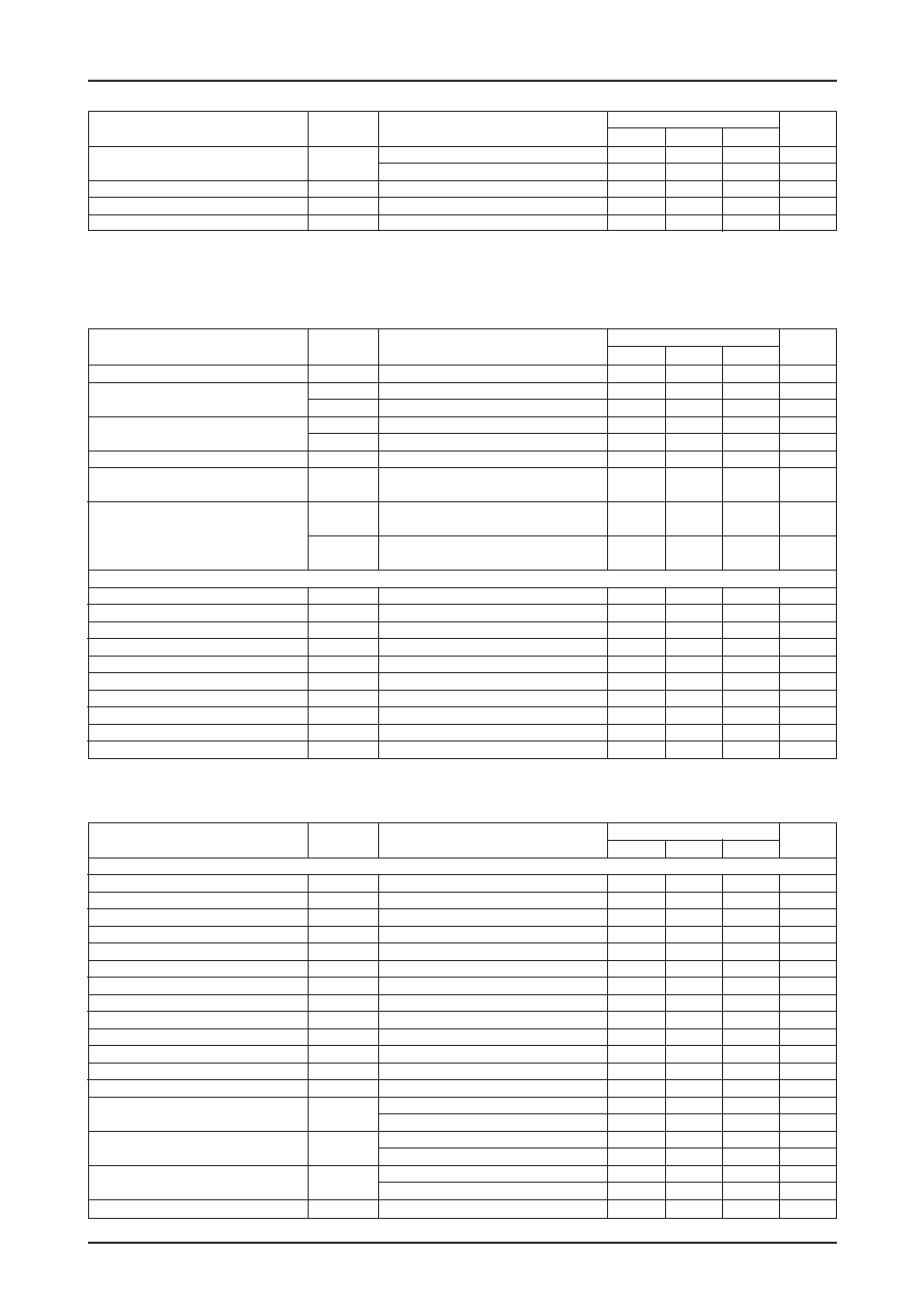
Ratings
Parameter
Symbol
Conditions
min
typ
max
Unit
RDY width (corrected output read)
tWDRDY
RDY (BUSWD=L 8bits)
60
210
nS
RDY ((BUSWD=H 16bits)
300
490
nS
DACK to DREQ delay
tDREQ
DREQ, DACK
260
nS
DMA cycle wait
tCYDM
RD, DREQ
420
nS
RD low-level width (DMA)
tWRDM
RD
300
nS
Notes: Application designs must take the RDY signal output delay into consideration if the RDY signal is used as the CPU bus wait signal.
If the RDY signal is not used, (that is, if no wait states are inserted) the value of the RD low-level width will be 250ns (minimum).
[LC72711LW]
Allowable Operating Ranges at Ta=-40 to +85°C, VSS=0V
Ratings
Parameter
Symbol
Conditions
min
typ
max
Unit
Supply voltage
VDD
2.7
3.6
V
High-level input voltage
VIH1
A0/CL, A1/CE, A2/DI, RST, STNBY
0.7VDD
5.5
V
VIH2
DACK, WR, RD, CS, SP, BUSWD, A3, IOCNT1, IOCNT2
0.7VDD
VDD
V
Low-level input voltage
VIL1
Pins for which VIH1 applies
VSS
0.3VDD
V
VIL2
Pins for which VIH2 applies
VSS
0.3VDD
V
Oscillator frequency
FOSC
This IC operates with a frequency precision of ±250 ppm
7.2
MHz
XIN input sensitivity
VXI
With a sine wave input to XIN, capacitor coupling,
400
900
mVrms
VDD=+2.7 to +3.6V
VMPX1
With a 100% modulated composite signal input to
120
350
mVrms
Input amplitude
MPXIN, VDD=+3.3V
VMPX2
With a 100% modulated composite signal input to
120
180
mVrms
MPXIN, VDD=+2.7V
[Serial I/O]
Clock low-level period
tCL
A0/CL
0.7
S
Clock high-level period
tCH
A0/CL
0.7
S
Data setup time
tSU
A0/CL, A2/DI
0.7
S
Data hold time
tHD
A0/CL, A2/DI
0.7
S
CE wait time
tEL
A0/CL, A1/CE
0.7
S
CE setup time
tES
A0/CL, A1/CE
0.7
S
CE hold time
tEH
A0/CL, A1/CE
0.7
S
Data latch change time
tLC
A1/CE
0.7
S
Data output time
tDDO
DO, A0/CL
277
555
nS
CRC4 change time
tCRC
CRC4, A0/CL
0.7
S
[LC72711LW]
Allowable Operating Ranges: Parallel Interface at Ta=-40 to +85°C, VSS=0V
Ratings
Parameter
Symbol
Conditions
min
typ
max
Unit
[Parallel I/O]
Address to RD setup
tSARD
A0/CL, A1/CE, A2/DI, A3, RD
20
nS
RD to address hold
tHARD
A0/CL, A1/CE, A2/DI, A3, RD, tWRDL=>250ns
-20
nS
RD low-level width
tWRDL1
RD
280
nS
RD low-level width (when RDY is used)
tWRDL2
RD
100
nS
RD cycle wait
tCYRD
A0/CL, A1/CE, A2/DI, A3, RD
150
nS
RDY width (Register read)
tWRDY
RDY
60
230
nS
RD data hold
tRDH
RD, DATn
0
nS
Address to WR setup
tSAWR
A0/CL, A1/CE, A2/DI, A3, WR
20
nS
WR to address hold
tHAWR
A0/CL, A1/CE, A2/DI, A3, WR
20
nS
WR cycle wait
tCYWR
A0/CL, A1/CE, A2/DI, A3, WR
150
nS
WR low-level width
tWWRL
WR
200
nS
WR data hold
tWDH
WR, DATn
0
nS
RDY output delay
tDRDY
RD, RDY
0
50
nS
Corrected output RD width
tWDRD1
RD (BUSWD=L 8bits)
300
nS
RD (BUSWD=H 16bits)
540
nS
Corrected output RD width
tWDRD2
RD (BUSWD=L 8bits)
100
nS
(when RDY is used)
RD (BUSWD=H 16bits)
300
nS
RDY width (corrected output read)
tWDRDY
RDY (BUSWD=L 8bits)
60
230
nS
RDY ((BUSWD=H 16bits)
300
490
nS
DACK to DREQ delay
tDREQ
DREQ, DACK
260
nS
Continued on next page.
相关PDF资料 |
PDF描述 |
|---|---|
| LC72713W | SPECIALTY CONSUMER CIRCUIT, PQFP64 |
| LC72713W | SPECIALTY CONSUMER CIRCUIT, PQFP64 |
| LC72714W | SPECIALTY CONSUMER CIRCUIT, PQFP64 |
| LC72714W | SPECIALTY CONSUMER CIRCUIT, PQFP64 |
| LC72715PW | SPECIALTY CONSUMER CIRCUIT, PQFP64 |
相关代理商/技术参数 |
参数描述 |
|---|---|
| LC72711LW-E | 制造商:ON Semiconductor 功能描述:DARC DECODE-LSI - Trays |
| LC72711LWHS-E | 功能描述:射频接收器 RoHS:否 制造商:Skyworks Solutions, Inc. 类型:GPS Receiver 封装 / 箱体:QFN-24 工作频率:4.092 MHz 工作电源电压:3.3 V 封装:Reel |
| LC72711W | 制造商:SANYO 制造商全称:Sanyo Semicon Device 功能描述:Mobile FM Multiplex Broadcast DARC Receiver IC |
| LC72711W_12 | 制造商:SANYO 制造商全称:Sanyo Semicon Device 功能描述:Mobile FM Multiplex Broadcast (DARC) Receiver IC |
| LC72713W | 制造商:未知厂家 制造商全称:未知厂家 功能描述: |
发布紧急采购,3分钟左右您将得到回复。