- 您现在的位置:买卖IC网 > PDF目录30732 > LC74735NW (SANYO SEMICONDUCTOR CO LTD) ON-SCREEN DISPLAY IC, PQFP80 PDF资料下载
参数资料
| 型号: | LC74735NW |
| 厂商: | SANYO SEMICONDUCTOR CO LTD |
| 元件分类: | 画面叠加 |
| 英文描述: | ON-SCREEN DISPLAY IC, PQFP80 |
| 封装: | SQFP-80 |
| 文件页数: | 15/52页 |
| 文件大小: | 300K |
| 代理商: | LC74735NW |
第1页第2页第3页第4页第5页第6页第7页第8页第9页第10页第11页第12页第13页第14页当前第15页第16页第17页第18页第19页第20页第21页第22页第23页第24页第25页第26页第27页第28页第29页第30页第31页第32页第33页第34页第35页第36页第37页第38页第39页第40页第41页第42页第43页第44页第45页第46页第47页第48页第49页第50页第51页第52页
No. 7545-22/52
LC74735NW
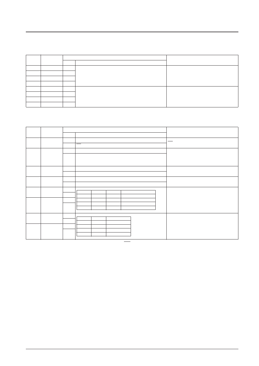
Command 25 (Output control 3 setting command)
First byte
Second byte
DA0 to 7
Register
Content
Notes
State
Function
7
—
1
6
—
0
Command 2 identification code
5
—
1
Output control
4
—
0
3
—
0
2
—
1
Extended command 5 identification code
1
0
1
DA0 to 7
Register
Content
Notes
State
Function
7
CEHSL
0
Normal operation
CE pin
1
CE pin held fixed at the high level
6
TOKSL
0
Normal mode
Transmissive mode
1
The color specified at address 0 in color table No. 1 is displayed
in the transmissive state.
5
VIPSL
0
Falling edge detection
Selects the detection polarity for the VSYNC signal.
1
Rising edge detection
4
OTMD2
0
Output off state (always low)
CLKOUT pin (pin 18)
1
Normal output
Output control
3
OTMD1
0
1
0
2
OTMD0
1
QRM1
0
1
0
QRM0
1
A0 to 17 output selection
Transmissive mode specification
OTMD2
OTMD1
OTMD0
Output
0
Normal
0
1
RGB No. 1
0
1
0
RGB No. 2
0
1
High-impedance state
ROM selection when character output is specified
in QVGA mode
QRM1
QRM0
ROM selection
0
ROM1
0
1
ROM2
1
0
ROM3
1
ROM4
*: This register is set to the all bits zero state when the IC is reset by the RST pin.
When RGB No. 1 or RGB No. 2 is selected:
The A17 to 9 output is set to the RD2 to BD0 three-value output. (Supported by connecting external resistors.)
* It will not be possible to use external ROM in this case. (Only internal ROM can be used.)
No. 1: RGB = 000 = Black only. Here the output will go to the high-impedance state giving the middle level due to the external resistor.
For areas other than the display area, the output will be at the low level.
No. 2: When any individual color is zero, the output will go to the high-impedance state giving the middle level due to the external resistor.
For areas other than the display area, the output will be at the low level.
相关PDF资料 |
PDF描述 |
|---|---|
| LC74735NW | ON-SCREEN DISPLAY IC, PQFP80 |
| LC74735W | ON-SCREEN DISPLAY IC, PQFP80 |
| LC74736PT | ON-SCREEN DISPLAY IC, PQFP100 |
| LC74751 | ON-SCREEN DISPLAY IC, PDIP22 |
| LC7475 | ON-SCREEN DISPLAY IC, PDIP22 |
相关代理商/技术参数 |
参数描述 |
|---|---|
| LC74735NWH-8A17-E | 制造商:ON Semiconductor 功能描述: |
| LC74735NWH-9817-E | 功能描述:显示驱动器和控制器 RoHS:否 制造商:Panasonic Electronic Components 工作电源电压:2.7 V to 5.5 V 最大工作温度: 安装风格:SMD/SMT 封装 / 箱体:QFN-44 封装:Reel |
| LC74735NWS-9817-E | 制造商:ON Semiconductor 功能描述:ON-SCREEN DISPLAY CONTROL - Trays 制造商:ON Semiconductor 功能描述:FTRAY / ON-SCREEN DISPLAY CONTROL |
| LC74735W | 制造商:未知厂家 制造商全称:未知厂家 功能描述: |
| LC74736PT | 制造商:SANYO 制造商全称:Sanyo Semicon Device 功能描述:CMOS IC On-Screen Display Controller |
发布紧急采购,3分钟左右您将得到回复。