- 您现在的位置:买卖IC网 > PDF目录30733 > LC74782 (SANYO SEMICONDUCTOR CO LTD) ON-SCREEN DISPLAY IC, PDIP24 PDF资料下载
参数资料
| 型号: | LC74782 |
| 厂商: | SANYO SEMICONDUCTOR CO LTD |
| 元件分类: | 画面叠加 |
| 英文描述: | ON-SCREEN DISPLAY IC, PDIP24 |
| 封装: | SDIP-24 |
| 文件页数: | 9/16页 |
| 文件大小: | 183K |
| 代理商: | LC74782 |
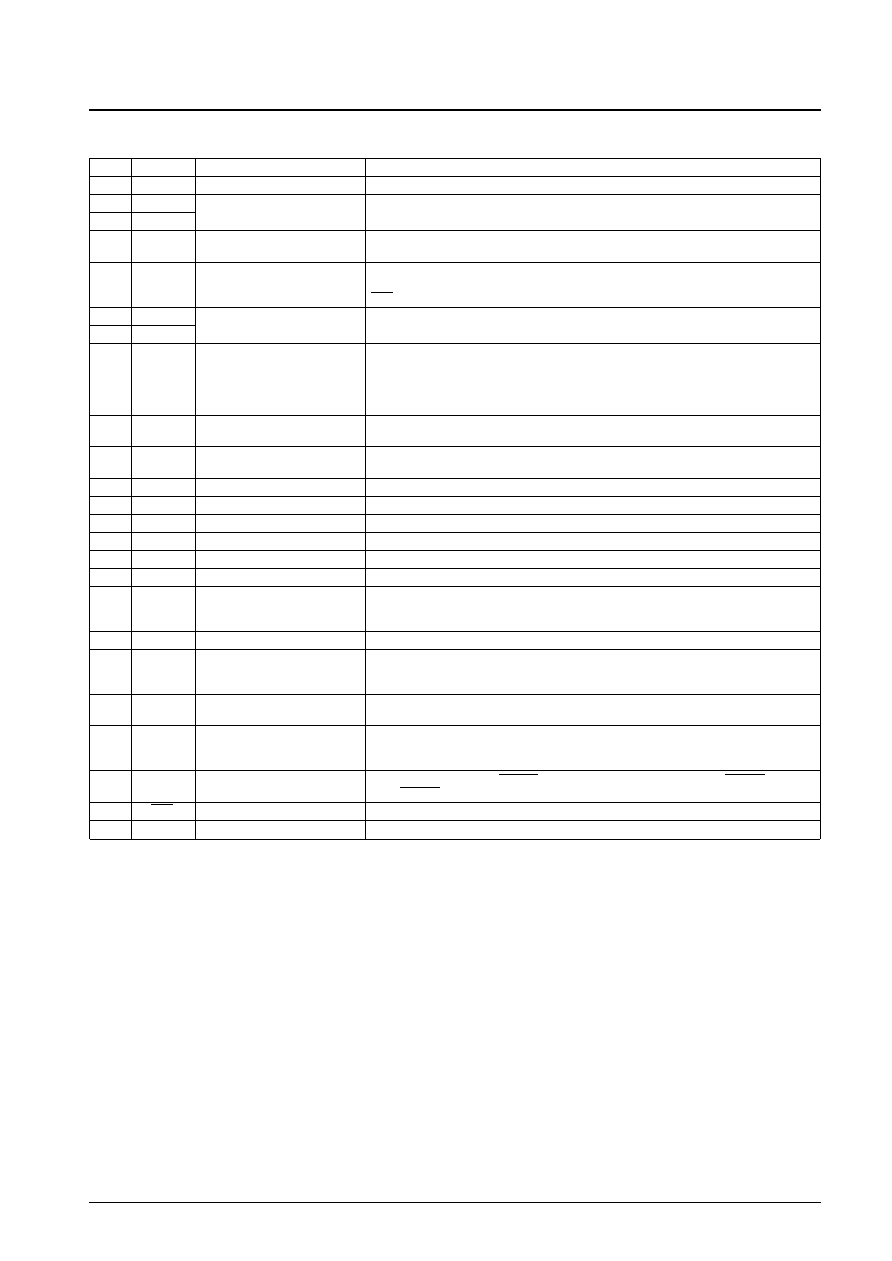
Pin Functions
No. 4989-2/16
LC74782, 74782M
Pin No.
Symbol
Function
Description
1
VSS1
Ground
Ground connection (digital system ground)
2
XtalIN
Crystal oscillator connection
Used to connect the crystal oscillator and capacitor used to generate the internal
3
XtalOUT
synchronization signal, or to input an external clock (2fsc or 4fsc).
4
CTRL1
Crystal oscillator input switching
Switches between external clock input mode and crystal oscillator mode.
Low = crystal oscillator mode, high = external clock mode
Outputs the blank signal (the OR of the character and border signals). (Outputs a composite
5
BLANK
Blanking output
sync signal when MOD0 is high.) Outputs the crystal oscillator clock during reset (when the
RST pin is low), but can be set up to not output this signal by microprocessor command.
6
OSCIN
LC oscillator connection
Connections for the coil and capacitor that form the oscillator that generates the character
7
OSCOUT
output dot clock.
Outputs the character signal. (Functions as the external synchronization signal discrimination
signal output pin when MOD0 is high, and outputs the state of the judgment as to whether the
8
CHARA
Character output
external synchronization signal is present or not. Outputs a high level when the synchronization
signal is present.) Outputs the dot clock (LC oscillator) during reset, but can be set up to not
output this signal by microprocessor command.
9
CS
Enable input
Serial data input enable input. Serial data input is enabled when low. A pull-up resistor is built in
(hysteresis input).
10
SCLK
Clock input
Serial data input clock input.
A pull-up resistor is built in (hysteresis input).
11
SIN
Data input
Serial data input. A pull-up resistor is built in (hysteresis input).
12
VDD2
Power supply
Composite video signal level adjustment power supply pin (analog system power supply).
13
CVOUT
Video signal output
Composite video signal output
14
NC
Must be either connected to ground or left open.
15
CVIN
Video signal input
Composite video signal input
16
VDD1
Power supply
Power supply (+5 V: digital system power supply)
Video signal input for the built-in sync separator circuit (Used for either horizontal
17
SYNIN
Sync separator circuit input
synchronization signal or composite sync signal input when the built-in sync separator circuit is
not used.)
18
SEPC
Sync separator circuit bias voltage
Built-in sync separator circuit bias voltage monitor pin
Built-in sync separator circuit composite sync signal output. (When MOD1 is high, outputs a high
19
SEPOUT
Composite sync signal output
level during internal synchronization and a low level during external synchronization.) (Outputs
the SYNIN input signal when the internal sync separator circuit is not used.)
20
SEPIN
Vertical synchronization
Inputs a vertical synchronization signal created by integrating the SEPOUT pin output signal. An
signal input
integrator must be attached at the SEPOUT pin. This pin must be tied to VDD1 if unused.
The setting indicated by this pin takes priority in switching between the NTSC, PAL, PAL-M and
21
CTRL2
NTSC/PAL-M switching input
PAL-N formats. A low level selects NTSC after a reset. The microprocessor command NTSC,
PAL, PAL-M, or PAL-N setting is valid. High = PAL-M format.
22
CTRL3
SEPIN input control
Controls whether or not the VSYNC signal is input to the SEPIN input. Low = VSYNC input,
high = VSYNC not input.
23
RST
Reset input
System reset input. A pull-up resistor is built in (hysteresis input).
24
VDD1
Power supply (+5 V)
Power supply (+5 V: digital system power supply)
相关PDF资料 |
PDF描述 |
|---|---|
| LC74782M | ON-SCREEN DISPLAY IC, PDSO24 |
| LC74782M | ON-SCREEN DISPLAY IC, PDSO24 |
| LC74783 | ON-SCREEN DISPLAY IC, PDIP24 |
| LC74783M | ON-SCREEN DISPLAY IC, PDSO24 |
| LC74783M | ON-SCREEN DISPLAY IC, PDSO24 |
相关代理商/技术参数 |
参数描述 |
|---|---|
| LC74782M | 制造商:SANYO 制造商全称:Sanyo Semicon Device 功能描述:On-screen Display Controller LSI for VCR Products |
| LC74782M-8A13-E | 制造商:ON Semiconductor 功能描述: |
| LC74782M-9011-E | 功能描述:显示驱动器和控制器 RoHS:否 制造商:Panasonic Electronic Components 工作电源电压:2.7 V to 5.5 V 最大工作温度: 安装风格:SMD/SMT 封装 / 箱体:QFN-44 封装:Reel |
| LC74783 | 制造商:SANYO 制造商全称:Sanyo Semicon Device 功能描述:On-screen Display Controller LSI for VCR Products |
| LC74783M | 制造商:SANYO 制造商全称:Sanyo Semicon Device 功能描述:On-screen Display Controller LSI for VCR Products |
发布紧急采购,3分钟左右您将得到回复。