- 您现在的位置:买卖IC网 > PDF目录30734 > LC749402BG COLOR SIGNAL CONVERTER, PBGA96 PDF资料下载
参数资料
| 型号: | LC749402BG |
| 元件分类: | 颜色信号转换 |
| 英文描述: | COLOR SIGNAL CONVERTER, PBGA96 |
| 封装: | 6 X 6 MM, BGA-96 |
| 文件页数: | 9/11页 |
| 文件大小: | 86K |
| 代理商: | LC749402BG |
LC749402BG
No.A1618-7/11
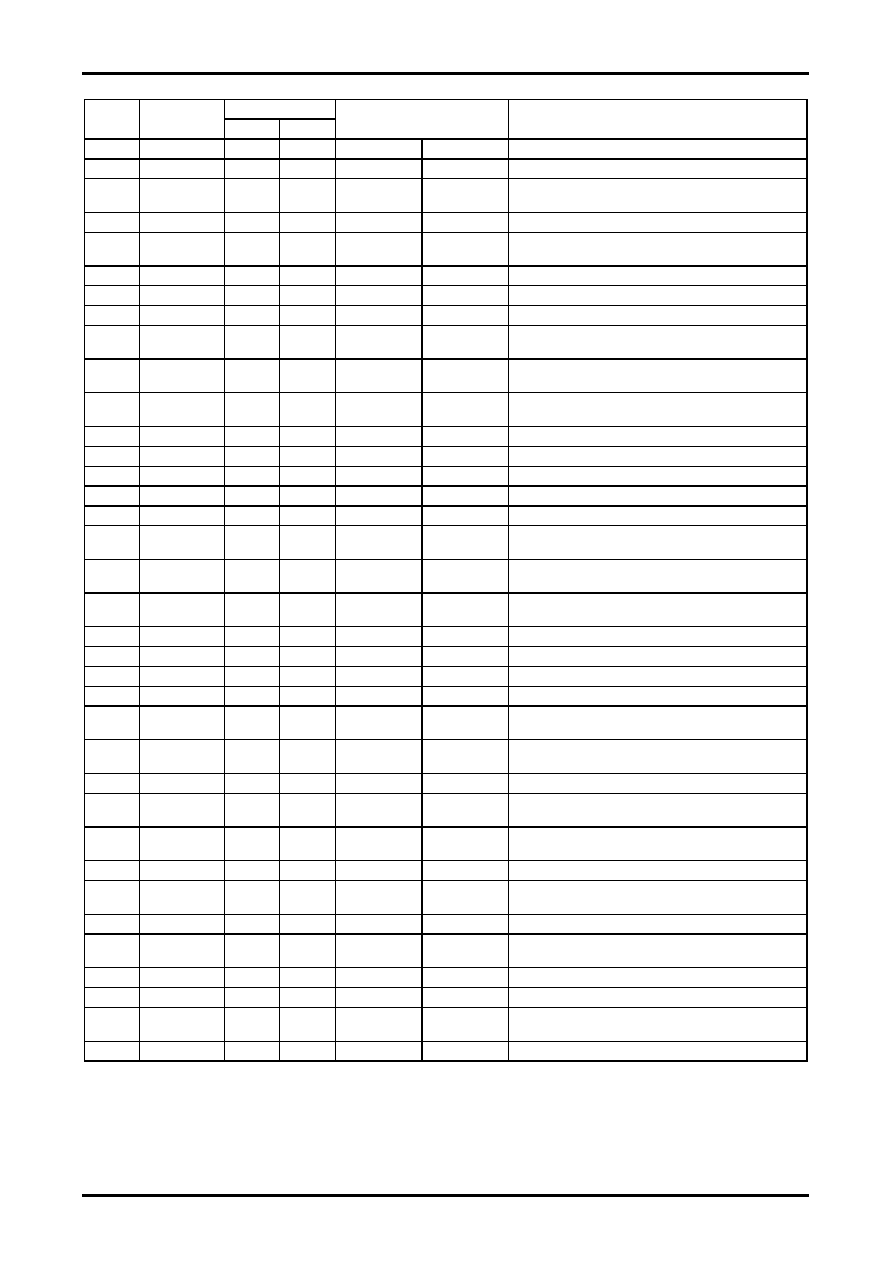
Continued from preceding page.
In/output format
Pin No.
Pin symbol
I/O
Format
Connecting
destination
Remarks
E1
DCRIN5
I
C
CMOS
Digital
R/Cr video. Connect this pin to GND when not to be used.
E2
DCRIN6
I
C
CMOS
Digital
R/Cr video. Connect this pin to GND when not to be used.
E3
DCRIN7
I
C
CMOS
Digital
R/Cr video (MSB).
Connect this pin to GND when not to be used.
E4
DVSS
P
-
GND
Digital
E7
PDWN
I
A
CMOS
Digital
“H” power down.
Connect this pin to GND when not to be used.
E8
DROUT4
O
F
CMOS
Digital
R/Cr video
E9
DROUT3
O
F
CMOS
Digital
R/Cr video
E10
DROUT2
O
F
CMOS
Digital
R/Cr video (6-bit output mode, LSB)
F1
DYGIN0
I
C
CMOS
Digital
G/Y/656 video (LSB).
Connect this pin to GND when not to be used.
F2
DYGIN1
I
C
CMOS
Digital
G/Y/656 video.
Connect this pin to GND when not to be used.
F3
DYGIN2
I
C
CMOS
Digital
G/Y/656 video.
Connect this pin to GND when not to be used.
F4
DVSS
P
-
GND
Digital
F7
DVDD_CORE
P
-
Core voltage
Digital
F8
DROUT1
O
F
CMOS
Digital
R/Cr video
F9
DROUT0
O
F
CMOS
Digital
R/Cr video (8-bit output mode, LSB)
F10
DCKO
O
G
CMOS
Digital
Video clock
G1
DYGIN3
I
C
CMOS
Digital
G/Y/656 video.
Connect this pin to GND when not to be used.
G2
DYGIN4
I
C
CMOS
Digital
G/Y/656 video.
Connect this pin to GND when not to be used.
G3
DYGIN5
I
C
CMOS
Digital
G/Y/656 video.
Connect this pin to GND when not to be used.
G4
DVSS
P
-
GND
Digital
G5
SCS_I2SEL
I
A
CMOS
Digital
SIO chip enable/I
2C slave address switching
G6
SIOSEL
I
C
CMOS
Digital
“L”: I
2C slave, ”H”: 4-wire SIO
G7
DVDD_CORE
P
-
Core voltage
Digital
G8
DHSO/SP2
O
F
CMOS
Digital
Horizontal synchronizing signal/start pulse signal for source
driver
G9
DVSO/FLM2
O
F
CMOS
Digital
Vertical synchronizing signal/start pulse signal for gate
driver
G10
DDEO
O
F
CMOS
Digital
Data enable signal
H1
DYGIN6
I
C
CMOS
Digital
G/Y/656 video.
Connect this pin to GND when not to be used.
H2
DYGIN7
I
C
CMOS
Digital
G/Y/656 video (MSB).
Connect this pin to GND when not to be used.
H3
DVSS
P
-
GND
H4
DCBIN6
I
C
CMOS
Digital
B/Cb/C video.
Connect this pin to GND when not to be used.
H5
DVSI
I
C
CMOS
Digital
Vertical synchronizing signal
H6
OSDBL
I
C
CMOS
Digital
Data enable signal for external OSD.
Connect this pin to GND when not to be used.
H7
FLM
O
F
CMOS
Digital
Start pulse signal for gate driver
H8
DVDD_CORE
P
-
Core voltage
Digital
H9
DEXR
O
F
CMOS
Digital
Reversed video signal output for DTR. Low output when the
DTR is OFF.
H10
POL
O
F
CMOS
Digital
Voltage polarity selection signal for source driver
Continued on next page.
相关PDF资料 |
PDF描述 |
|---|---|
| LC749402BG | COLOR SIGNAL CONVERTER, PBGA96 |
| LC749450NW | SPECIALTY CONSUMER CIRCUIT, PQFP208 |
| LC749460W | SPECIALTY CONSUMER CIRCUIT, PQFP256 |
| LC749460W | SPECIALTY CONSUMER CIRCUIT, PQFP256 |
| LC74950BG | SPECIALTY CONSUMER CIRCUIT, PBGA96 |
相关代理商/技术参数 |
参数描述 |
|---|---|
| LC749402BG-TLM-H | 功能描述:显示驱动器和控制器 RoHS:否 制造商:Panasonic Electronic Components 工作电源电压:2.7 V to 5.5 V 最大工作温度: 安装风格:SMD/SMT 封装 / 箱体:QFN-44 封装:Reel |
| LC749402PT | 制造商:SANYO 制造商全称:Sanyo Semicon Device 功能描述:CMOS IC Silicon gate LCD Picture Quality Improvement IC |
| LC749402PT-H | 功能描述:显示驱动器和控制器 RoHS:否 制造商:Panasonic Electronic Components 工作电源电压:2.7 V to 5.5 V 最大工作温度: 安装风格:SMD/SMT 封装 / 箱体:QFN-44 封装:Reel |
| LC749403BG | 制造商:SANYO 制造商全称:Sanyo Semicon Device 功能描述:Silicon gate LCD Picture Quality Improvement IC |
| LC749450NW | 制造商:SANYO 制造商全称:Sanyo Semicon Device 功能描述:Silicon Gate CMOS IC Digital RGB Image Processor IC |
发布紧急采购,3分钟左右您将得到回复。