- 您现在的位置:买卖IC网 > PDF目录30734 > LC74986NWF SPECIALTY CONSUMER CIRCUIT, PQFP144 PDF资料下载
参数资料
| 型号: | LC74986NWF |
| 元件分类: | 消费家电 |
| 英文描述: | SPECIALTY CONSUMER CIRCUIT, PQFP144 |
| 封装: | SQFP-144 |
| 文件页数: | 13/15页 |
| 文件大小: | 116K |
| 代理商: | LC74986NWF |
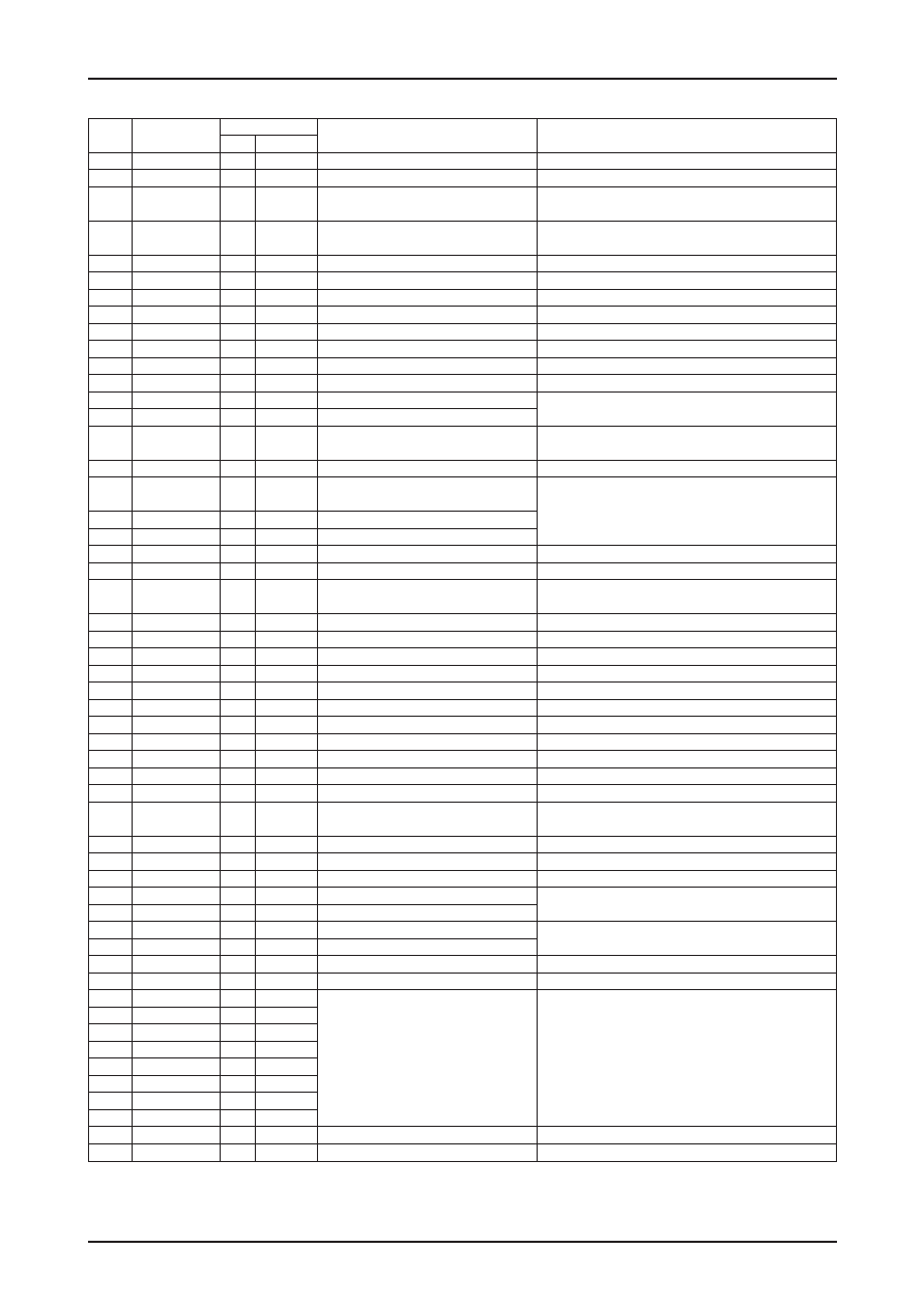
No.7713-7/15
LC74986NWF, 74986NWV
Pin
Symbol
I/O and type
Function
Notes
number
I/O
Type
1
DVSS
P
—
Digital system ground
2
PLLHIO
O
gqcio19
Input or external PLL divided clock output
The divider ratio can be set over the I2C bus.
3
CLKIO
O
gqcio20
Outputs the input clock
Has the same period as the input system. The output can be
inverted by a setting controllable over the I2C bus.
4
CLKIEN
I
gqcio02
Port A system input clock enable
This input is normally held fixed at the high level. (Positive
logic.)
5
CLKI
I
gqcio02
Port A system input clock
Input signal pixel clock
6
AVDD
P
—
Analog system power supply: 3.3V
Connect to DVDD2 if unused.
7
AVSS
P
—
Analog system ground
8
VCOCNT1
I
gqcio10
PLL VCO control voltage input
Connect to AVSS if unused.
9
VCORNG1
I
gqcio10
PLL range setting resistor connection
Connect to AVSS if unused.
10
PDO1
O
gqcio09
PLL phase comparator output
Leave open if unused.
11
DVDD1
P
—
Digital system power supply: 2.5V (1.8V)
12
DVSS
P
—
Digital system ground
13
SDA
B
gqcio22
I2C bus data
Used for setting internal registers and for reading out IC status.
14
SCL
I
gqcio03
I2C bus clock
Also used for OSD control and gamma correction settings.
15
I2CSEL
I
gqcio18
I2C bus slave address switching
Normally left open (slave address: 70h) or connected to
DVSS.
16
MUTE
I
gqcio02
Muting control
Inverted logic
17
AICS (VPBV)
I
gqcio03
Chip select or port B system vertical sync
Three-wire bus: use is optional.
signal
Only used for OSD control (Normally, the I2C bus is used.)
18
AIDA
I
gqcio03
Data
The AICS pin uses inverted logic.
19
AICK
I
gqcio03
Clock
VPBP can be used by setting a register.
20
RST
I
gqcio03
Initial reset
Inverted logic
21
PDOWN1
I
gqcio02
Power down
Normally held fixed at the high level (Used for testing.)
22
PDOWN2 (VPBV)
I
gqcio03
Power down or port B system vertical sync
(Used for testing.) VPBV can be used by setting a register.
signal
23
DVDD1
P
—
Digital system power supply: 2.5V (1.8V)
24
DVSS
P
—
Digital system ground
25
XTAL
I
gqcio02
Clock input for the detection functions
Connection for the fixed-frequency oscillator
26
DCLKI
I
gqcio02
Display clock input
Display processing pixel clock
27
DVDD1
P
—
Digital system power supply: 2.5V (1.8V)
28
DVSS
P
—
Digital system ground
29
DVSS
P
—
Digital system ground
30
DVSS
P
—
Digital system ground
31
VPBCK
I
gqcio02
Port B system input clock
Port B system input signal pixel clock
32
DVDD1
P
—
Digital system power supply: 2.5V (1.8V)
33
DVSS
P
—
Digital system ground
34
DCLK0
O
gqcio20
LCD panel module clock output
Has the same period as DCLKI.
Alternatively, may have 1/2 the period.
35
VPBH
I
gqcio03
Port B system horizontal sync signal
Port B system input horizontal sync signal
36
DVDD1
P
—
Digital system power supply: 2.5V (1.8V)
37
DVSS
P
—
Digital system ground
38
DEHO
O
gqcio19
FPD module horizontal enable
The polarity can be selected over the I2C bus.
39
DEVO
O
gqcio19
FPD module vertical enable
A composite signal can be output from DEVO.
40
HSO
O
gqcio19
FPD module horizontal sync signal
The polarity and pulse width can be set over the I2C bus.
41
VSO
O
gqcio19
FPD module vertical sync signal
A composite sync signal can be output from VSO.
42
DVDD2
P
—
Digital system power supply: 3.3V
43
DVSS
P
—
Digital system ground
44
ROUT0
O
gqcio19
FPD module R output
LSB
45
ROUT1
O
gqcio19
(The ROUT5:0 pins are used for 6-bit output.)
46
ROUT2
O
gqcio19
When 2-phase output is used, the first byte is data.
47
ROUT3
O
gqcio19
(MSB when 6-bit output is selected)
48
ROUT4
O
gqcio19
49
ROUT5
O
gqcio19
50
ROUT6
O
gqcio19
51
ROUT7
O
gqcio19
MSB
52
DVDD2
P
—
Digital system power supply: 3.3V
53
DVSS
P
—
Digital system ground
Pin Functions Items in parentheses apply to the LC74986NWV.
Continued on next page.
相关PDF资料 |
PDF描述 |
|---|---|
| LC74986NWV | SPECIALTY CONSUMER CIRCUIT, PQFP144 |
| LC749870LG | SPECIALTY CONSUMER CIRCUIT, PBGA64 |
| LC749870W | SPECIALTY CONSUMER CIRCUIT, PQFP64 |
| LC749880T | SPECIALTY CONSUMER CIRCUIT, PQFP120 |
| LC749880T | SPECIALTY CONSUMER CIRCUIT, PQFP120 |
相关代理商/技术参数 |
参数描述 |
|---|---|
| LC749870W | 制造商:SANYO 制造商全称:Sanyo Semicon Device 功能描述:Silicon gate NTSC/PAL/SECAM Digital Video Decoder |
| LC749880T | 制造商:SANYO 制造商全称:Sanyo Semicon Device 功能描述:Silicon gate Image controller LSI for LCD-TV |
| LC749880T-E | 功能描述:视频 IC RoHS:否 制造商:Fairchild Semiconductor 工作电源电压:5 V 电源电流:80 mA 最大工作温度:+ 85 C 封装 / 箱体:TSSOP-28 封装:Reel |
| LC74FCT162245T | 制造商:未知厂家 制造商全称:未知厂家 功能描述: |
| LC74FCT16245T | 制造商:未知厂家 制造商全称:未知厂家 功能描述:Dual 8-bit Bus Transceiver |
发布紧急采购,3分钟左右您将得到回复。