- 您现在的位置:买卖IC网 > PDF目录30735 > LC75343M 2 CHANNEL(S), TONE CONTROL CIRCUIT, PDSO36 PDF资料下载
参数资料
| 型号: | LC75343M |
| 元件分类: | 音频控制 |
| 英文描述: | 2 CHANNEL(S), TONE CONTROL CIRCUIT, PDSO36 |
| 封装: | 0.375 INCH, MFP-36 |
| 文件页数: | 6/28页 |
| 文件大小: | 413K |
| 代理商: | LC75343M |
第1页第2页第3页第4页第5页当前第6页第7页第8页第9页第10页第11页第12页第13页第14页第15页第16页第17页第18页第19页第20页第21页第22页第23页第24页第25页第26页第27页第28页
No. 6867-14/28
LC75343M
Continued from preceding page.
Pin No.
Pin Name
Function
Equivalent circuit
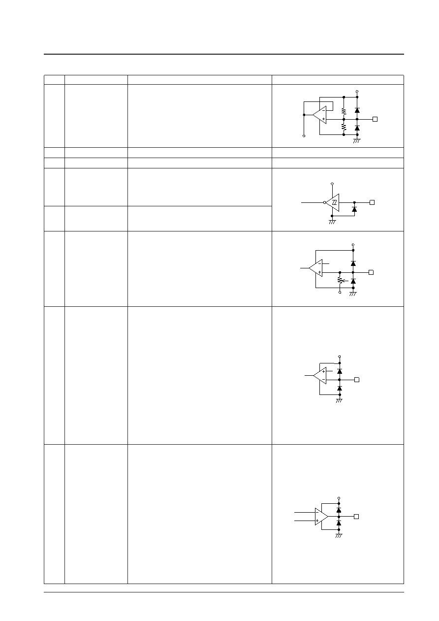
Connect a capacitor of a few tens of F between Vref and
AVSS (VSS) as a analog ground 0.5 × VDD voltage
generator, current ripple countermeasure.
19
Vref
VDD
Vref
VDD
Ground pin
3
VSS
Power supply pin
35
VDD
Chip enable pin
Data is written to the internal latch and the analog switches
are operated when the level changes from high to low.
Data transfer is enabled when the level is high.
2CE
VDD
INP
Vref
General-purpose op-amp specifications
Non-inverted input pins of general-purpose op-amp
When not used, leave open.
ATT control specifications
Non-inverted input pins for ATT.
3-band specifications
Non-inverted input pins for ATT.
Always leave these pins open.
6
32
LINP
RINP
VDD
INM
General-purpose op-amp specifications
Non-inverted input pins of general-purpose op-amp.
When not used, connect these pins to the L(R) OPOUT pins.
(Connected between pin 5 and pin 4)
(Connected between pin 33 and pin 34)
ATT control specifications
Op-amp inverted input pins for ATT.
Connected to L(R) OPOUT pins.
(Connected between pin 5 and pin 4)
(Connected between pin 33 and pin 34)
3-band specifications
Inverted input pins of ATT op-amp.
Connected to L(R) OPOUT pins.
(Connected between pin 5 and pin 4)
(Connected between pin 33 and pin 34)
5
33
LINM
RINM
VDD
OPOUT
General-purpose op-amp specifications
General-purpose op-amp output pins.
When not used, connect these pins to the L(R) INM pins.
(Connected between pin 5 and pin 4)
(Connected between pin 33 and pin 34)
ATT control specifications
Op-amp output pins for ATT.
Connected to L(R) INM pins.
(Connected between pin 5 and pin 4)
(Connected between pin 33 and pin 34)
3-band specifications
ATT op-amp output pins.
(Connected to L(R) INM pins.
(Connected between pin 5 and pin 4)
(Connected between pin 33 and pin 34)
4
34
LOPOUT
ROPOUT
Serial data pins and clock input pin for control
1
36
DI
CL
相关PDF资料 |
PDF描述 |
|---|---|
| LC75344M | 2 CHANNEL(S), VOLUME CONTROL CIRCUIT, PDSO10 |
| LC75345M | 2 CHANNEL(S), TONE CONTROL CIRCUIT, PDSO36 |
| LC75345M | 2 CHANNEL(S), TONE CONTROL CIRCUIT, PDSO36 |
| LC75347E | 6 CHANNEL(S), TONE CONTROL CIRCUIT, PQFP44 |
| LC75347E | 6 CHANNEL(S), TONE CONTROL CIRCUIT, PQFP44 |
相关代理商/技术参数 |
参数描述 |
|---|---|
| LC75343M-MPB-E | 制造商:ON Semiconductor 功能描述:ELECTRONIC VOLUME - Ammo Pack 制造商:ON Semiconductor 功能描述:Multimedia Misc 制造商:ON Semiconductor 功能描述:FNFLD / ELECTRONIC VOLUME |
| LC75343M-TLM-E | 功能描述:音频 DSP RoHS:否 制造商:Texas Instruments 工作电源电压: 电源电流: 工作温度范围: 安装风格: 封装 / 箱体: 封装:Tube |
| LC75344M | 制造商:SANYO 制造商全称:Sanyo Semicon Device 功能描述:2 CHANNEL VOLUME SYSTEM |
| LC75344MC-AH | 制造商:ON Semiconductor 功能描述:ELECTRONIC VOLUME - Tape and Reel |
| LC75344MC-D-AH | 制造商:ON Semiconductor 功能描述: 制造商:ON Semiconductor 功能描述:ELECTRONIC VOLUME |
发布紧急采购,3分钟左右您将得到回复。