- 您现在的位置:买卖IC网 > PDF目录30735 > LC7536M 2 CHANNEL(S), VOLUME CONTROL CIRCUIT, PDSO30 PDF资料下载
参数资料
| 型号: | LC7536M |
| 元件分类: | 音频控制 |
| 英文描述: | 2 CHANNEL(S), VOLUME CONTROL CIRCUIT, PDSO30 |
| 封装: | MFP-30 |
| 文件页数: | 7/10页 |
| 文件大小: | 107K |
| 代理商: | LC7536M |
No. 6089-6/10
LC7536M
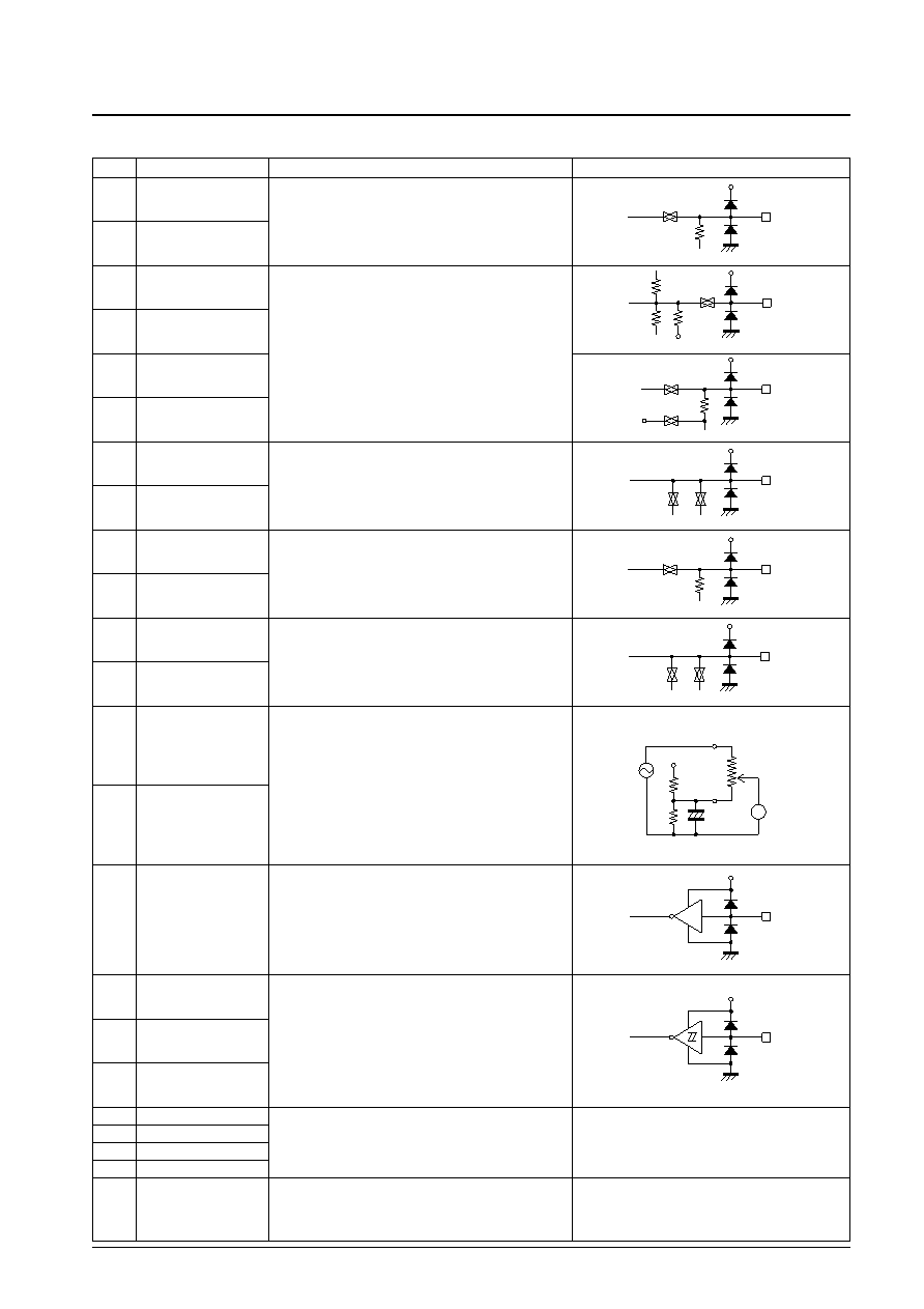
Pin Functions
Pin No.
Pin
Function
Equivalent circuit
5-dB step attenuator inputs
These inputs must be driven by low-impedance circuits.
2
L5dBIN
VDD
A11996
29
R5dBIN
Loudness circuit connections
Connect high-band compensation capacitors between the
CT1 and 5dBIN pins, and connect low-band compensation
capacitors between the CT2 and VM pins.
3
LCT1
CT2
VDD
A11997
CT1
VDD
A11998
28
RCT1
5-dB step attenuator outputs
These signals should be received by loads of about 47 k
to 1 M
.
5
L5dBOUT
VDD
A11999
26
R5dBOUT
1-dB step attenuator inputs
These inputs must be driven by low-impedance circuits.
7
L1dBIN
VDD
A12000
24
R1dBIN
1-dB step attenuator outputs
These signals should be received by loads of about 47 k
to 1 M
.
8
L1dBOUT
VDD
A12001
Common pins for the volume controls. The printed circuit
board pattern for these pins should be designed to have as
low an impedance as possible. Since LVM, RVM, and VSS
are not connected internally in the IC, they may be
connected to separate external circuits that meet their
individual specifications.
Since the capacitors between the VM pins and the power
supply when a single power supply is used become the
residual resistance components at maximum attenuation,
care is required in determining the values of these
capacitors.
9
LVM
22
RVM
V
VM
5dBIN
VDD
A12002
Selects the address code of data during formatted.
When this pin is connected to VDD, the IC accepts data
when the address code is 9, and when connected to VCC,
it accepts data when the address code is 8.
12
S
VDD
A12003
Inputs for the serial data that controls the IC. The input
signals must have an amplitude of 0 to 5 V.
17
CL
18
DI
19
CE
VDD
A12004
Power supply connections. These pins must be connected
to the corresponding power supply. Applications must be
designed so that VCC is not applied before VDD.
10
VEE
Unused pins. These pins must be left open.
1, 6, 11,
15, 16,
20, 25,
30
NC
23
R1dBOUT
13
VDD
14
VSS
21
VCC
4
LCT2
27
RCT2
相关PDF资料 |
PDF描述 |
|---|---|
| LC7536R | 2 CHANNEL(S), VOLUME CONTROL CIRCUIT, PDIP30 |
| LC75371M | 2 CHANNEL(S), TONE CONTROL CIRCUIT, PDSO36 |
| LC75372E | 2 CHANNEL(S), TONE CONTROL CIRCUIT, PQFP44 |
| LC75373E | 2 CHANNEL(S), TONE CONTROL CIRCUIT, PQFP44 |
| LC75374E | 2 CHANNEL(S), TONE CONTROL CIRCUIT, PQFP44 |
相关代理商/技术参数 |
参数描述 |
|---|---|
| LC7536R | 制造商:SANYO 制造商全称:Sanyo Semicon Device 功能描述:High Breakdown Voltage Serial Control Electronic Volume Control |
| LC7537 | 制造商:SANYO 制造商全称:Sanyo Semicon Device 功能描述:Electronic Volume Control System for Audio Equipment |
| LC75371M | 制造商:SANYO 制造商全称:Sanyo Semicon Device 功能描述:Car Stereo Electronic Tone and Volume Control |
| LC75372E | 制造商:SANYO 制造商全称:Sanyo Semicon Device 功能描述:Electronic Volume Control for Car Stereo Systems |
| LC75373E | 制造商:SANYO 制造商全称:Sanyo Semicon Device 功能描述:Electronic Volume Control for Car Stereo Systems |
发布紧急采购,3分钟左右您将得到回复。