- 您现在的位置:买卖IC网 > PDF目录30736 > LC7871NE SPECIALTY CONSUMER CIRCUIT, PQFP100 PDF资料下载
参数资料
| 型号: | LC7871NE |
| 元件分类: | 消费家电 |
| 英文描述: | SPECIALTY CONSUMER CIRCUIT, PQFP100 |
| 封装: | QFP-100 |
| 文件页数: | 6/19页 |
| 文件大小: | 299K |
| 代理商: | LC7871NE |
5. Channel Selection: Pins CH0 to CH15
The channel can be selected by controlling the values of the CH0 to CH15 pin input values. The logical OR is taken
with the microprocessor input register.
6. CD Graphics Monitor: The CDGM pin
The CDGM signal goes high when the LC7871E or LC7871NE receives, even once, any one of the page 11 CDG
instructions. Since the circuits are connected as soon as this signal goes high in the power on state, a reset will be
required when changing disks if this pin is used.
7. Video Output: The VIDEO pin
A composite video signal can be acquired from the VIDEO pin. The output level from the 8-bit D/A converter is
1.25 Vp-p. Therefore, an external 6 dB video amplifier is required to acquire a 1 Vp-p rated output.
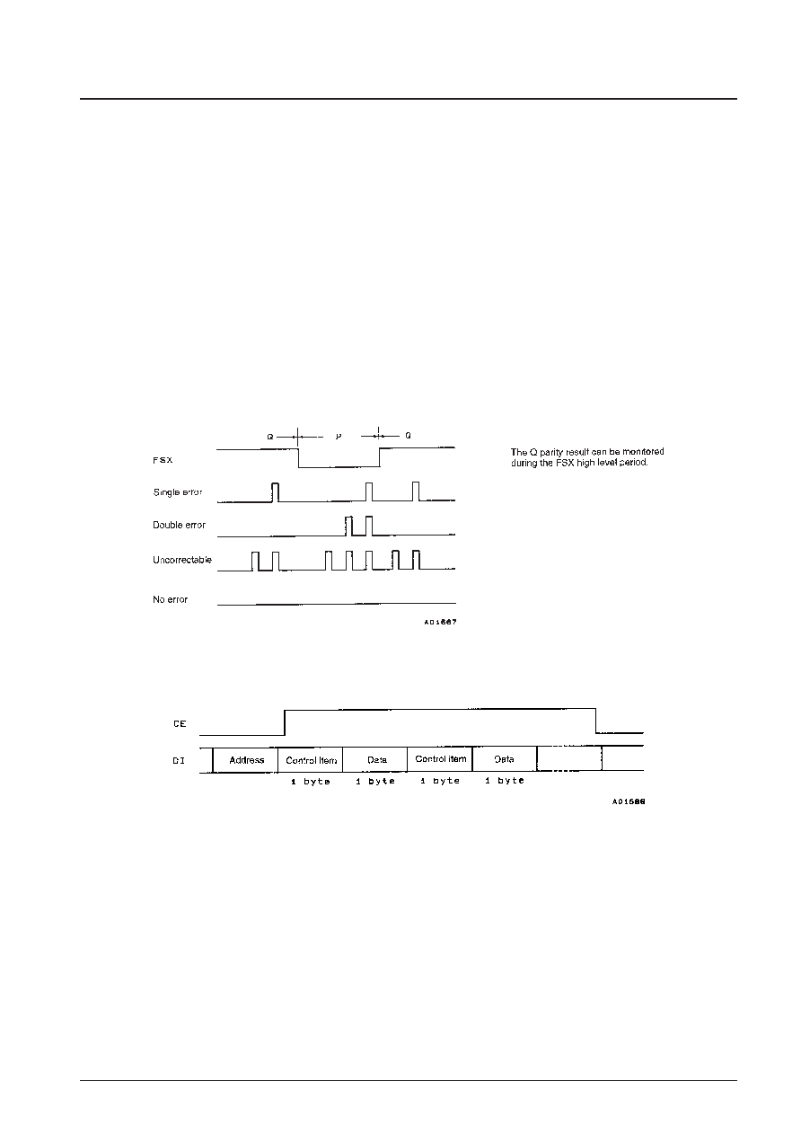
8. Error Flag Output: Pin EFLG and FSX
The error detection result can be monitored from the EFLG pin.
Microcontroller Interface (CCB bus)
1. 2N byte command input
Address (F4h): lsb [00101111] msb
Control item:
lsb [0---AAAA] msb
A = register number
Register 0 (mode setting)
Data: lsb [ABCDEFGH] msb.
The default is[00000110].
A = VRAM/BG
0: Display the contents of VRAM
1: Display the background color
B = TV/LINE
0: TV mode (Extended TV mode)
1: Line graphics mode
C = Disk command enable
0: Disk commands are accepted. MGC commands (microcontroller graphics commands,
executed by 19-byte command inputs) are executed between disk commands,
1: Disk commands are ignored and only MGC commands are executed.
No. 4861-14/19
LC7871E, 7871NE
相关PDF资料 |
PDF描述 |
|---|---|
| LC7872E | SPECIALTY CONSUMER CIRCUIT, PQFP64 |
| LC7874E | SPECIALTY CONSUMER CIRCUIT, PQFP64 |
| LC78835K | SPECIALTY CONSUMER CIRCUIT, PDIP24 |
| LC78835KM | SPECIALTY CONSUMER CIRCUIT, PDSO24 |
| LC78845Q | SPECIALTY CONSUMER CIRCUIT, PQFP48 |
相关代理商/技术参数 |
参数描述 |
|---|---|
| LC7872E | 制造商:Panasonic Industrial Company 功能描述:IC |
| LC7874E | 制造商:SANYO 制造商全称:Sanyo Semicon Device 功能描述:CD Graphics Decorder |
| LC7876E | 制造商:未知厂家 制造商全称:未知厂家 功能描述: |
| LC7880 | 制造商:SANYO 制造商全称:Sanyo Semicon Device 功能描述:16 bit D/A CONVERTER |
| LC7880M | 制造商:SANYO 制造商全称:Sanyo Semicon Device 功能描述:16 bit D/A CONVERTER |
发布紧急采购,3分钟左右您将得到回复。