- 您现在的位置:买卖IC网 > PDF目录39191 > LC78817M SERIAL INPUT LOADING, 16-BIT DAC, PDSO10 PDF资料下载
参数资料
| 型号: | LC78817M |
| 元件分类: | DAC |
| 英文描述: | SERIAL INPUT LOADING, 16-BIT DAC, PDSO10 |
| 封装: | MFP-10 |
| 文件页数: | 4/6页 |
| 文件大小: | 82K |
| 代理商: | LC78817M |
Pin Functions
Operating Description
1. Digital Audio Data Input
The digital audio data is a 16-bit signal in an msb-first twos complement format. The 16 bits of data are acquired in
synchronization with the rising edge of BCLK starting with the msb. See the timing chart for details.
2. Conversion (see Figure 1)
The LC78817 and LC78817M includes two independent D/A converter circuits, one each for channels one and two.
It adopts a dynamic level shifting conversion technique that uses a resistor-string D/A converter, a PWM (pulse
width modulation) D/A converter, and a level shifting D/A converter. After latching the 16 bits of digital audio data
(D15 to D0):
the upper 8 bits (D15 to D8) are input to the resistor-string D/A converter, and
the middle 4 bits (D7 to D4) are input to the PWM D/A converter, and
the lower 4 bits (D8 to D0) are input to the level-shifting D/A converter.
Resistor-string D/A converter
This is a D/A converter in which a total of 256 (= 28) unit-resistance resistors are connected in series and the
potential applied to the ends of that resistor string is voltage divided into 256 equal intervals. Of these resistor-
divided potentials, two adjacent potentials, V1 and V2, are selected by a switching circuit according to the value of
the upper 8 bits of the data. These two potentials are output to the PWM D/A converter. Note that these potentials
are related as follows:
V2 – V1 = (VH – VL)/256
PWM D/A converter
This is a 4-bit D/A converter that divides (by 16) the interval between the two potentials, V1 and V2, output by the
resistor-string D/A converter. This circuit outputs one or the other of the V1 and V2 potentials from the CH1OUT
(or CH2OUT) pin according to the value of the middle 4 bits of the data.
Level shifting D/A converter
This 4-bit D/A converter is implemented by connecting the variable resistors VRH and VRL in series at the ends of
the resistor-string D/A converter. The values of the VRH and VRL variable resistors are modified according to the
value of the low-order 4 bits of the data as follows:
— The value of VRH + VRL is held fixed regardless of the value of the data.
— The values of VRH and VRL are changed in R/256 unit steps (where R is the value of the resistor-string D/A
converter unit resistors) over the range zero to 15R/256.
This causes the resistor-string D/A converter V1 and V2 outputs to change in
V/256 steps (where V = (VH –
VL)/256) over the range 0 to 15
× V/256 according to the value of the lower 4 bits of the data.
No. 5107-4/6
LC78817, 78817M
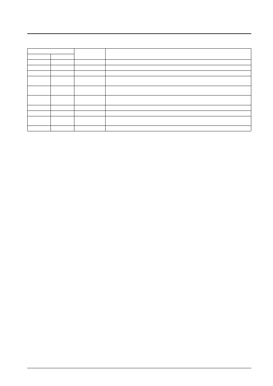
Pin No.
Symbol
Function and Operation
LC78817
LC78817M
1
CH1OUT
CH1 analog output (left channel)
2
VDD
Power supply voltage
—
3
NC
No connection
3
4
BCLK
Bit clock input
This pin inputs the clock used for bit serial input of the digital audio input data.
4
5
LRCK
L/R clock input
This pin inputs the signal that discriminates the left and right digital audio data signals.
5
6
DATA
Digital audio data input
This pin inputs data in an msb-first bit-serial format. (A twos complement representation is used.)
6
7
GND
Ground
—
8
NC
No connection
7
9
REFH
Reference voltage
Connect to ground through a capacitor.
8
10
CH2OUT
CH2 analog output (right channel)
相关PDF资料 |
PDF描述 |
|---|---|
| LC78817 | SERIAL INPUT LOADING, 16-BIT DAC, PDIP8 |
| LC78832M | SERIAL INPUT LOADING, 16-BIT DAC, PDSO20 |
| LC78833M | SERIAL INPUT LOADING, 16-BIT DAC, PDSO20 |
| LC78833V | SERIAL INPUT LOADING, 16-BIT DAC, PDSO24 |
| LC78834M | SERIAL INPUT LOADING, 18-BIT DAC, PDSO28 |
相关代理商/技术参数 |
参数描述 |
|---|---|
| LC7881M | 制造商:Panasonic Industrial Company 功能描述:IC |
| LC78820 | 制造商:未知厂家 制造商全称:未知厂家 功能描述:Audio Digital-to-Analog Converter |
| LC78820M | 制造商:未知厂家 制造商全称:未知厂家 功能描述:Audio Digital-to-Analog Converter |
| LC7883 | 制造商:SANYO 制造商全称:Sanyo Semicon Device 功能描述:LC7883M |
| LC78832M | 制造商:SANYO 制造商全称:Sanyo Semicon Device 功能描述:16-Bit D/A Converter LSI with On-Chip Digital Filters |
发布紧急采购,3分钟左右您将得到回复。