- 您现在的位置:买卖IC网 > PDF目录30736 > LC8213K SPECIALTY CONSUMER CIRCUIT, PQFP80 PDF资料下载
参数资料
| 型号: | LC8213K |
| 元件分类: | 消费家电 |
| 英文描述: | SPECIALTY CONSUMER CIRCUIT, PQFP80 |
| 封装: | QFP-80 |
| 文件页数: | 4/5页 |
| 文件大小: | 171K |
| 代理商: | LC8213K |
Functional Description
Encoding method
Conforms to the MH, MR, and MMR encoding methods of the ITU-T T.4 and T.6 recommendations, which are the
standards for G3 and G4 facsimile.
Processing modes
Processing is performed in block units, and the number of lines processed can be set to be up to 64k lines. Processing can
also be performed in single line units. The LC8213K includes two FIFO systems, one for encoding and one for decoding,
so it is also possible to perform encoding and decoding alternately in units of several lines. In encoding mode, data is
read out sequentially from the image memory start address loaded into a register and encoded. The encoded data is
written to the encoding FIFO. The CPU is interrupted after the specified number of lines of data have been encoded. In
decoding mode, encoded data is read out of the decoding FIFO and decoded. The image data is recovered and written to
image memory. The CPU is interrupted after the specified number of lines of data have been decoded or a decoding error
occurs.
Line skip mode
This is a mode in which the amount of code for a completely white line is set to half the set minimum number of
transmission bits. A line skip bit, which is used to recognize that a line is completely white, is added after the EOL code,
and fill bits are added so that the amount of code is one half the minimum number of transmission bits. For lines that are
not all white, the normal coded data is transmitted after the line skip bit.
No. 5753-4/5
LC8213K
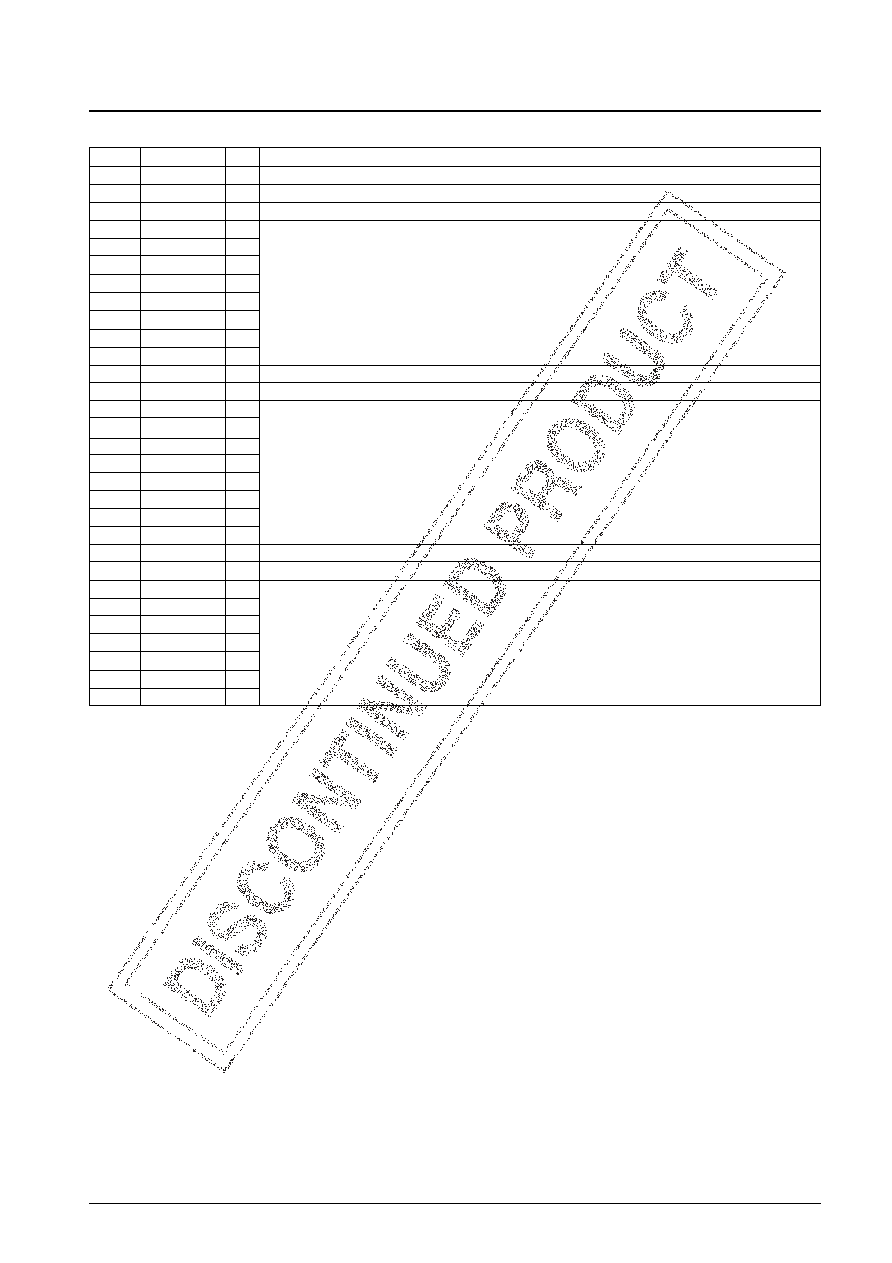
Pin No.
Pin name
I/O
Function
51
DTC
O
DMA transfer complete signal
52
VSS
P
Ground
53
VDD
P
Power supply
54
MA23
O
55
MA22
O
56
MA21
O
57
MA20
O
Upper 8 bits of the image memory address
58
MA19
O
59
MA18
O
60
MA17
O
61
MA16
O
62
MA/MD15
B
Lower 16 bits of the image memory address/16-bit data bus
63
VSS
P
Ground
64
MA/MD14
B
65
MA/MD13
B
66
MA/MD12
B
67
MA/MD11
B
Lower 16 bits of the image memory address/16-bit data bus
68
MA/MD10
B
69
MA/MD9
B
70
MA/MD8
B
71
MA/MD7
B
72
VSS
P
Ground
73
VDD
P
Power supply
74
MA/MD6
B
75
MA/MD5
B
76
MA/MD4
B
77
MA/MD3
B
Lower 16 bits of the image memory address/16-bit data bus
78
MA/MD2
B
79
MA/MD1
B
80
MA/MD0
B
Continued from preceding page.
相关PDF资料 |
PDF描述 |
|---|---|
| LC82151 | SPECIALTY CONSUMER CIRCUIT, PQFP144 |
| LC82161B-E | SPECIALTY CONSUMER CIRCUIT, PQFP208 |
| LC8220 | SPECIALTY CONSUMER CIRCUIT, PQFP160 |
| LC82210 | SPECIALTY CONSUMER CIRCUIT, PQFP100 |
| LC82220 | SPECIALTY CONSUMER CIRCUIT, PQFP128 |
相关代理商/技术参数 |
参数描述 |
|---|---|
| LC8214 | 制造商:SANYO 制造商全称:Sanyo Semicon Device 功能描述:Facsimile Controller |
| LC82141 | 制造商:SANYO 制造商全称:Sanyo Semicon Device 功能描述:Facsimile Controller |
| LC82150 | 制造商:SANYO 制造商全称:Sanyo Semicon Device 功能描述:CMOS LSI |
| LC82151 | 制造商:SANYO 制造商全称:Sanyo Semicon Device 功能描述:Single-Chip Facsimile Controller |
| LC821621-E | 制造商:ON Semiconductor 功能描述:VOIP PROCESSOR - Trays |
发布紧急采购,3分钟左右您将得到回复。