- 您现在的位置:买卖IC网 > PDF目录30736 > LC82151 SPECIALTY CONSUMER CIRCUIT, PQFP144 PDF资料下载
参数资料
| 型号: | LC82151 |
| 元件分类: | 消费家电 |
| 英文描述: | SPECIALTY CONSUMER CIRCUIT, PQFP144 |
| 封装: | SQFP-144 |
| 文件页数: | 7/8页 |
| 文件大小: | 64K |
| 代理商: | LC82151 |
No. 5601-7/8
LC82151
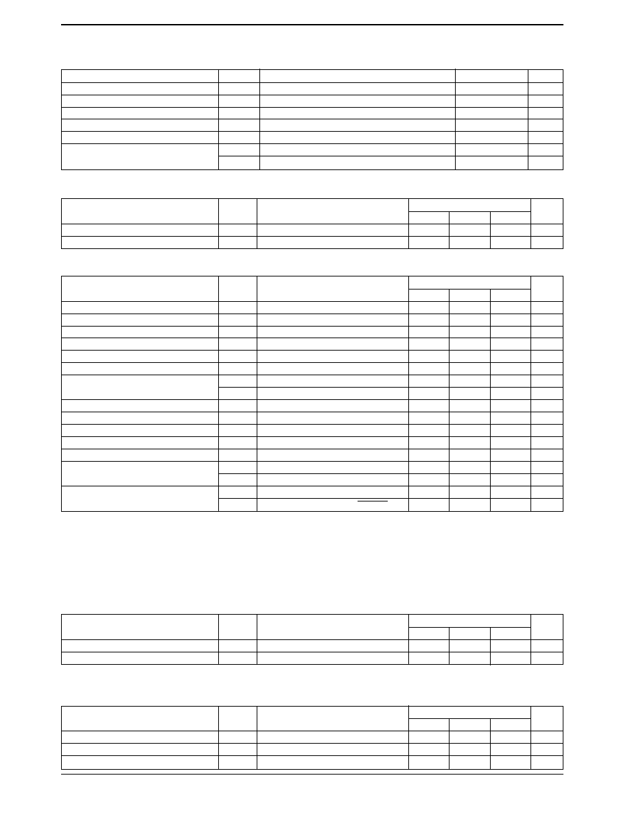
Specifications
Absolute Maximum Ratings at Ta = 25°C, VSS = 0 V
Parameter
Symbol
Conditions
Ratings
Unit
Maximum supply voltage
VDD max
–0.3 to +7.0
V
Input and output voltage
VI, VO
–0.3 to VDD +0.3
V
Allowable power dissipation
Pd max
Ta ≤ 70°C
550
mW
Operating temperature
Topr
–30 to +70
°C
Storage temperature
Tstg
–55 to +125
°C
Soldering temperature
Manual soldering (3 seconds)
350
°C
Reflow soldering (10 seconds)
235
°C
Parameter
Symbol
Conditions
Ratings
Unit
min
typ
max
Supply voltage
VDD
4.5
5.5
V
Input voltage
VIN
0VDD
V
Allowable Operating Ranges at Ta = –30 to +70°C, VSS = 0 V
Parameter
Symbol
Conditions
Ratings
Unit
min
typ
max
Input high-level voltage
VIH1
2.2
V
Input low-level voltage
VIL1
0.8
V
Input leakage current
IL
–10
+10
A
Output high-level voltage
VOH
IOH = –4mA
2.4
V
Output low-level voltage
VOL
IOL = 4mA
0.4
V
Output leakage current
IOZ
When outputs are high impedance
–10
+10
A
Charge pump output current
IPOZ
PHASEO = 2 V
7
15
27
mA
INOZ
PHASEO = 2 V
–8
–15
–28
mA
Vref input voltage
VREF
VDD/2
V
Vref impedance
VREF
1M
Input voltage range
VIA
RXA, PGCI
VDD × 0.2
VDD × 0.8
V
Operating voltage range
VOA
TXA, PGCO
VDD × 0.2
VDD × 0.8
V
Output impedance
RO
TXA, PGCO
7.0
k
Oscillator frequency
fCLK1
XTAL1, XTAL2, CLKIN
29.4912
MHz
fCLK2
ROSC1, ROSC 2
32.768
kHz
Current drain
IDD1
Operating
100
mA
IDD2
In backup mode, VDD = 2.5 V, BACKUP = 0
5A
Electrical Characteristics at Ta = –30 to +70°C, VDD = 4.5 to 5.5 V
Power on Timing
Applications must control the timing of the power on sequence carefully. Although AVSS and VSS are completely
isolated internally in the LC82151, AVDD and VDD are connected through the substrate. This means that there must be
no potential difference between AVDD and VDD. Also, the power supply voltage rise and fall times must be under 3 ms.
Parameter
Symbol
Conditions
Ratings
Unit
min
typ
max
Resolution
6
bit
Reference resistors value
DAREFL, DAREFH
5.0
k
Analog Characteristic
D/A Converter
Parameter
Symbol
Conditions
Ratings
Unit
min
typ
max
Resolution
8
bit
Linearity error
±1
LSB
Differential linearity error
±1
LSB
A/D Converter at an ATAP potential of 4.2 V
A/D Converter
相关PDF资料 |
PDF描述 |
|---|---|
| LC82161B-E | SPECIALTY CONSUMER CIRCUIT, PQFP208 |
| LC8220 | SPECIALTY CONSUMER CIRCUIT, PQFP160 |
| LC82210 | SPECIALTY CONSUMER CIRCUIT, PQFP100 |
| LC82220 | SPECIALTY CONSUMER CIRCUIT, PQFP128 |
| LC8230 | SPECIALTY CONSUMER CIRCUIT, PQFP100 |
相关代理商/技术参数 |
参数描述 |
|---|---|
| LC821621-E | 制造商:ON Semiconductor 功能描述:VOIP PROCESSOR - Trays |
| LC82162BL-E | 制造商:ON Semiconductor 功能描述:VOIP PROCESSOR - Trays |
| LC82162B-R1000-E | 制造商:ON Semiconductor 功能描述:VOIP PROCESSOR - Trays 制造商:ON Semiconductor 功能描述:Processors - Application Specialized |
| LC8220 | 制造商:SANYO 制造商全称:Sanyo Semicon Device 功能描述:JPEG Still Color Image Compression/Decompression LSI |
| LC82-2001G | 制造商:SEI Stackpole Electronics Inc 功能描述: |
发布紧急采购,3分钟左右您将得到回复。